TRI to display new Wafer Inspection and Metrology solution
Test Research, will join SEMICON Taiwan held at Taipei Nangang Exhibition Center, Hall 1 – 4F from September 4 - 6, 2024. OmniMeasure, TRI's SEMI inspection partner, will be joining TRI's booth #N0990.
Attendees are encouraged to visit TRI's booth to learn more about AI-powered AOI solutions for the Semiconductor and Advanced Packaging Industry. TRI has SEMI Inspection solutions for Advanced WLP/PLP and SEMI Back-End Package processes.
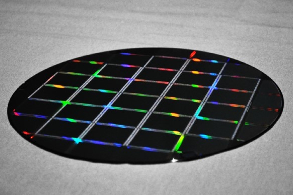
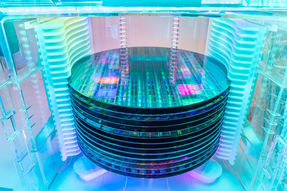
TRI will be exhibiting the new Wafer Inspection Platform, TR7950Q SII, featuring a 25MP camera with 2.5 μm resolution and a 12MP camera with 0.55um microlens for high-resolution 2D/3D DFF inspection and AI-powered inspection algorithms. The TR7950Q SII is suitable for the Wafer Macroscopic 3D Inspection and micro measurement metrology. The TR7950Q SII can inspect Advanced WLP, Wafer Frame, Patterned Wafer, Wafer Bumping, WLCSP, through-silicon via (TSV), and more. The TR7950Q SII can inspect TSV at ultra-high speeds thanks to the TSV module from OmniMeasure. TSV Metrology functions: sensing TSV depth, trench depth, oxide, nitride, PR, and PI film thickness.
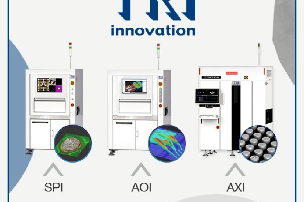
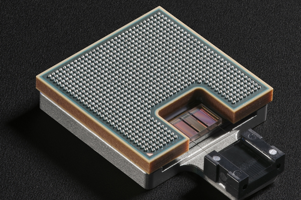
TRI will also showcase the latest back-end inspection solutions, TR7007Q SII-S and TR7700Q SII-S. The TR7007Q SII-S can inspect Mini-LED, C4 bumps (~100 μm Ø), and 008004 paste inspection applications. The AI-powered 3D SEMI AOI, TR7700Q SII-S, can inspect die, wire diameters of up to 15 μm (0.6 mil), SiP, underfill, bumps, and more. The lineup will also include an X-ray Inspection Demo Station. TRI's SEMI AXI solutions can inspect C4 bumps and Cu pillars.
Patterned Wafer TSV Metrology Wafer Frame Wafer Bumping Wire/Die Bonding
OmniMeasure will display the TGV (Through Glass Via) 3D Viewer, a TGV metrology tool that employs non-contact tomography measurement to view cross-sections of the glass via easily. The TGV viewer can also measure side wall angles without needing SEM.
Visit TRI's Booth No. N0990 at SEMICON Taiwan 2024 to learn more about TRI's SEMI applications and the latest inspection innovations for the Semiconductor and Advanced Packaging Industry.

