
Gauss Labs releases AI-based Virtual Metrology solution, Panoptes VM 2.0
SK hynix expands adoption of Gauss Labs's solution to etching process in addition to thin film deposition process.
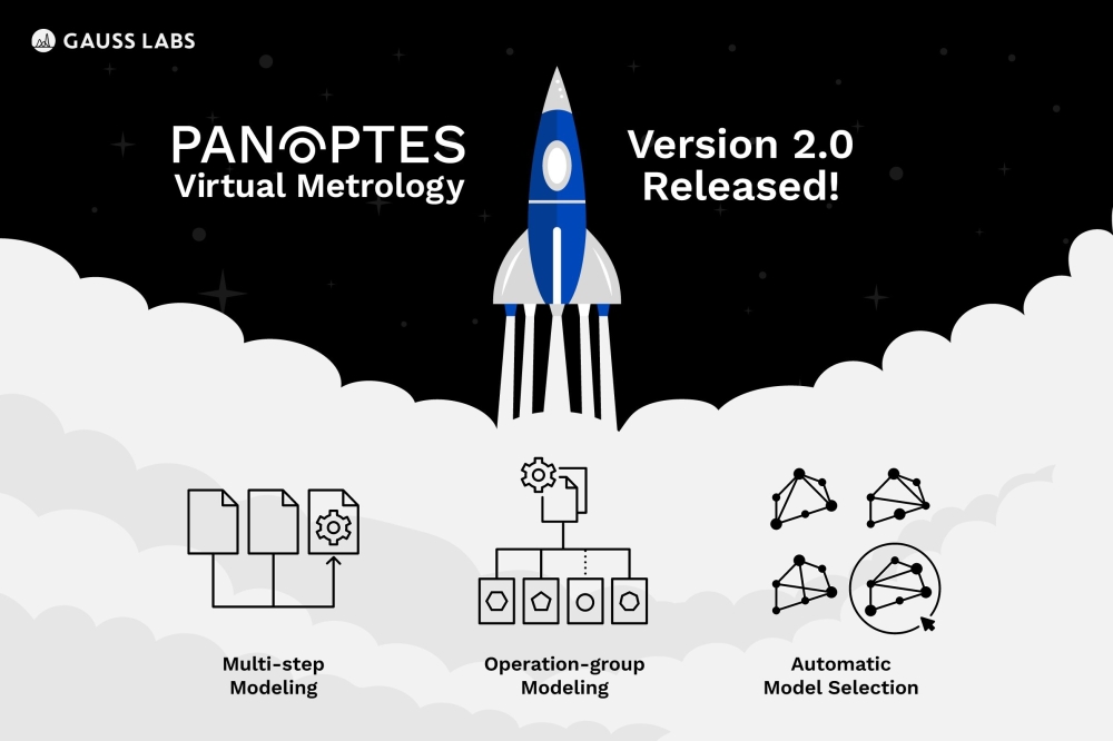
Gauss Labs has released the second version of its AI-based virtual metrology* solution, Panoptes VM 2.0.
Panoptes VM provides all-wafer measurement data in real-time by predicting process outcomes from sensor data. By applying this solution, it is possible to predict the process results of all products without physical full-scale measurement, significantly reducing time and resources.
Gauss Labs said that Panoptes VM 2.0 is making a new leap forward with new modeling features including the Multi-Step Modeling, Operation-Group Modeling and Automatic Model Selection. With these new features, the prediction accuracy and usability have been greatly improved, compared to the previous version.
Gauss Labs, an industrial AI company invested by SK hynix, first launched Panoptes VM 1.0 in November 2022. The system has been deployed to the thin film deposition process at SK hynix's high-volume manufacturing fabs since December 2022. By integrating the virtual measurement results from Panoptes VM with APC, SK hynix improved process variability by approximately 29% and also enhanced yield rate.
SK hynix plans to expand the application to APC use case. With the new Multi-Step Modeling feature, it expects to cover the etching process effectively. This new feature creates prediction models using data from not only the current step but also previous steps to improve the accuracy of VM predictions which is especially critical for etching process.
Panoptes VM 2.0 also provides the Operation-Group Modeling that allows the users to group data from similar operations for more effective modeling even when the data is scarce and the Automatic Model Selection, which supports multi-algorithm architecture and automatically selects the best performing model based on data characteristics to further improve the accuracy of VM as well as usability.
Gauss Labs, headquartered in Silicon Valley, was founded in 2020 with the vision of "revolutionizing manufacturing with AI" and has focused on "developing AI solutions for manufacturing data intelligence (MDI)."
Mike Kim, Chief Executive Officer of Gauss Labs, said, "Our concerted efforts over the past four years are now creating meaningful impact in the semiconductor industry, the most advanced manufacturing sector. Equipped with our state-of-the-art industrial AI technology, we will continue our march towards the global industrial AI market."


