
NEO Semiconductor outlines the development of its 3D X-AI Chip
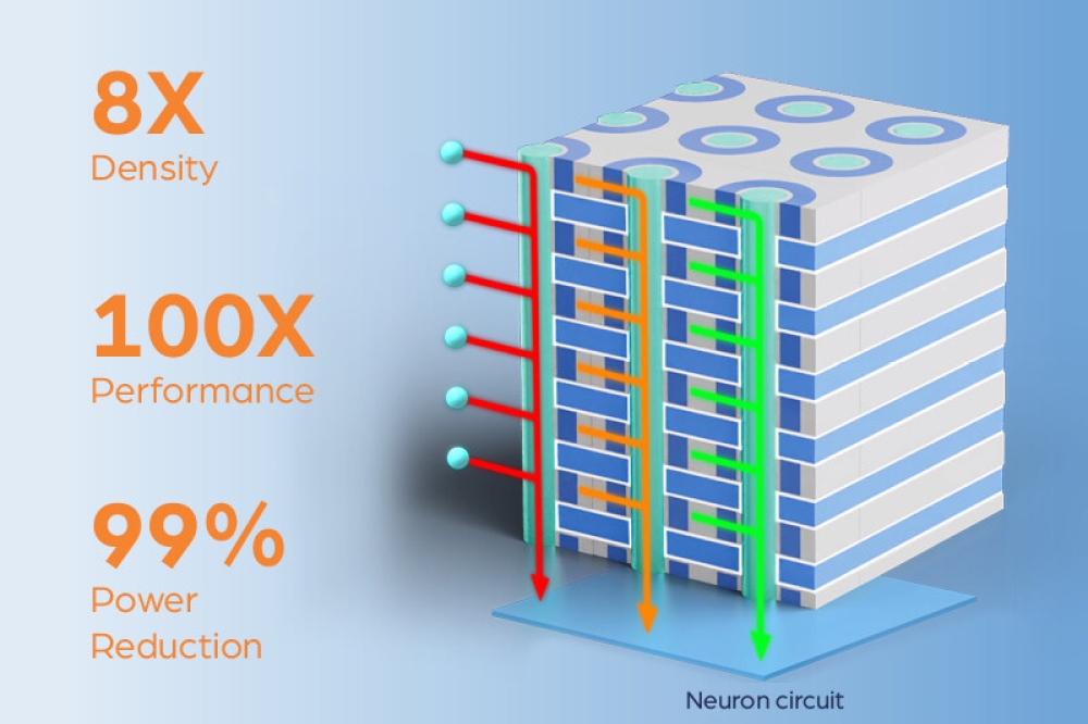
The new 3D X-AI Chip accelerates AI performance by 100X and reduces power consumption by 99%.
NEO Semiconductor, a leading developer of innovative technologies for 3D NAND flash memory and 3D DRAM, has announced the development of its 3D X-AI™ chip technology, targeted to replace the current DRAM chips inside high bandwidth memory (HBM) to solve data bus bottlenecks by enabling AI processing in 3D DRAM. 3D X-AI can reduce the huge amount of data transferred between HBM and GPUs during AI workloads. NEO's innovation is set to revolutionize the performance, power consumption, and cost of AI Chips for AI applications like generative AI.
NEO’s 3D X-AI Chip uses 3D memory to perform AI operations. It reduces huge amount of data transferred between HBM and GPU. Set to revolutionize the performance, power consumption, and cost of AI Chips for AI applications like generative AI.
AI Chips with NEO's 3D X-AI technology can achieve:
100X Performance Acceleration: contains 8,000 neuron circuits to perform AI processing in 3D memory.
99% Power Reduction: minimizes the requirement of transferring data to the GPU for calculation, reducing power consumption and heat generation by the data bus.
8X Memory Density: contains 300 memory layers, allowing HBM to store larger AI models.
"Current AI Chips waste significant amounts of performance and power due to architectural and technological inefficiencies," said Andy Hsu, Founder & CEO of NEO Semiconductor. "The current AI Chip architecture stores data in HBM and relies on a GPU to perform all calculations. This separated data storage and data processing architecture makes the data bus an unavoidable performance bottleneck. Transferring huge amounts of data through the data bus causes limited performance and very high power consumption. 3D X-AI can perform AI processing in each HBM chip. This can drastically reduce the data transferred between HBM and GPU to improve performance and reduce power consumption dramatically."
A single 3D X-AI die includes 300 layers of 3D DRAM cells with 128 Gb capacity and one layer of neural circuit with 8,000 neurons. According to NEO's estimation, this can support up to 10 TB/s of AI processing throughput per die. Using twelve 3D X-AI dies stacked with HBM packaging can achieve 120 TB/s processing throughput, resulting in a 100X performance increase.
"The application of 3D X-AI technology can accelerate the development of emerging AI use cases and promote the creation of new ones," said Jay Kramer, President of Network Storage Advisors. "Harnessing 3D X-AI technology to create the next generation of optimized AI Chips will spark a new era of innovation for AI Apps."


