Loading...
News Article

VEECO announces agreement with IBM

News

Veeco’s WaferStorm wet processing system to enable essential cleaning processes in hybrid bonding for IBM.

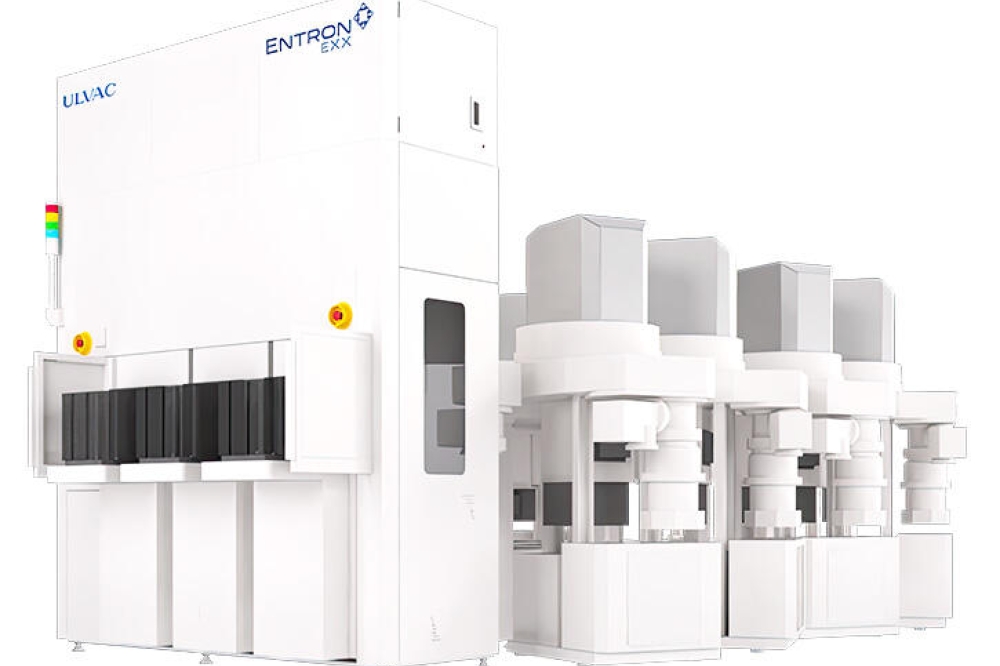
Veeco Instruments has announced that IBM selected the WaferStorm Wet Processing System for Advanced Packaging applications and has entered into a joint development agreement to explore advanced packaging applications using multiple wet processing technologies from Veeco. Under the agreement, the Waferstorm Wet Processing System will be installed at facilities at the Albany NanoTech Complex in Albany, NY, where IBM and other ecosystem partners are driving leading-edge R&D in advanced packaging and chiplet technologies.

The WaferStorm system enables crucial hybrid bonding cleaning processes such as resist strip, temporary bonding strip, and pre-bond cleaning with low defectivity thresholds at 40nm and 60nm. TheWaferStorm Wet Processing System’s ImmJET multi-wafer immersion and high-pressure spray technology can perform multiple processes on one flexible platform that can handle multiple wafer sizes and thicknesses with minimal hardware modifications.

“The collaboration with IBM illustrates Veeco’s commitment to partnering with leading device manufacturers at the forefront of critical emerging technologies including cloud and AI innovation,” commented Mathew Abraham, Veeco’s Vice President of Wet Processing Products. “Our innovative high throughput platform with industry-leading cost of ownership, powered by our proprietary ImmJET solvent technology, propels Advanced Packaging like never before and allows for superior process capabilities and cost-effectiveness. We’re keen to strengthen our relationship with IBM, a major tech pioneer pushing the limits of Advanced Packaging adoption.”

Due to its exceptional flexibility, Veeco’s WaferStorm system is the industry choice for critical wet processing applications in the advanced packaging, MEMS, RF, data storage, and photonics markets. The system supports a wide range of processes, including metal lift-off, photoresist, flux clean, scrubber, and TSV cleaning. With its process performance record and low cost of ownership, the WaferStorm system helps to ensure optimal results for photoresist strip and dry film strip applications, making it an ideal choice for customers keen on innovation.

Semiconductor Industry Network of Community Colleges launch
Researchers show that computer chips have the potential to become even smaller
Texas Instruments signs preliminary CHIPS Act agreement
RK Logistics Group acquires Tempe’ supply chain assets
Seoul Semiconductor achieves No.1 position in Display LEDs
ACC receives $7.5 million grant for semiconductor training
NSF awards RIT nearly $3 million to advance semiconductor technologies
Movellus joins the Silicon Catalyst In-Kind Partner Ecosystem
NEO Semiconductor outlines the development of its 3D X-AI Chip
IIT Guwahati develops ‘LEAP’
SK hynix signs Preliminary Memorandum of Terms with U.S. Department of Commerce
VEECO announces agreement with IBM
Gauss Labs releases AI-based Virtual Metrology solution, Panoptes VM 2.0
Akeana exits stealth mode
Exyte selects LTIMindtree
TRI to display new Wafer Inspection and Metrology solution
Advanced CMOS design sets 'new benchmark' in ultra-fast sensors
Industry to address child care needs
EU project ARCTIC joins quantum forces
Advantest celebrates 25th anniversary of V93000 SoC Test Platform
Advanced packaging in Europe: Swissbit hosts EuroPAT Workshop 2024
Introducing the N-332 - Vacuum Compatible Nanopositioning Stage family
ACM Research strengthens its fan-out panel level packaging portfolio
Imec demonstrates logic and DRAM structures using High NA EUV Lithography
Yongjiang Laboratory orders Reactive Ion Beam Trimming equipment from scia Systems
Paving the way for the semiconductor future
Government scheme helps UK chip start-ups raise £10 million
Renesas completes acquisition of Altium
Greene Tweed highlights Chemraz 541
Intel acts to 'accelerate progress'
Infineon reports slight increase in revenue and earnings in Q3 FY 2024
New partnership brings semiconductor manufacturing to Central Valley
×
Search the news archive

To close this popup you can press escape or click the close icon.
Logo
×
  • 1st January 1970
  • 1st January 1970
  • 1st January 1970
  • 1st January 1970
  • 1st January 1970
  • 1st January 1970
  • 1st January 1970
  • 1st January 1970
  • View all news 22645 more articles
Logo
×
Register - Step 1

You may choose to subscribe to the Silicon Semiconductor Magazine, the Silicon Semiconductor Newsletter, or both. You may also request additional information if required, before submitting your application.


Please subscribe me to:


You chose the industry type of "Other"

Please enter the industry that you work in: