ESMC breaks ground on Dresden fab

ESMC – a joint venture between TSMC, Robert Bosch GmbH, Infineon Technologies AG and NXP Semiconductors N.V. – recently held a groundbreaking ceremony to officially mark the initial phase of land preparation for its first semiconductor fab in Dresden, Germany.
The event brought together government officials, customers, suppliers, business partners and academia to celebrate a milestone in establishing what will be the EU’s first-ever FinFET-capable pure-play foundry.
Distinguished guests included president of the European Commission Ursula von der Leyen, German Chancellor Olaf Scholz, and Saxony Minister President Michael Kretschmer and Lord Mayor of Dresden, Dirk Hilbert. In a demonstration of dedicated support, during the event, President von der Leyen announced that the European Commission has approved, under EU State aid rules, a €5 billion German measure to support European Semiconductor Manufacturing Company (ESMC) in the construction and operation of the semiconductor fab.
"Together with our partners, Bosch, Infineon and NXP, we are building our Dresden facility to meet the semiconductor needs of the rapidly growing European automotive and industrial sectors,” said TSMC Chairman & CEO C.C. Wei. “With this state-of-the-art manufacturing facility, we will bring TSMC’s advanced manufacturing capabilities within reach of our European customers and partners, which will stimulate economic development within the region and drive technological advancements across Europe."
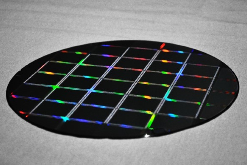
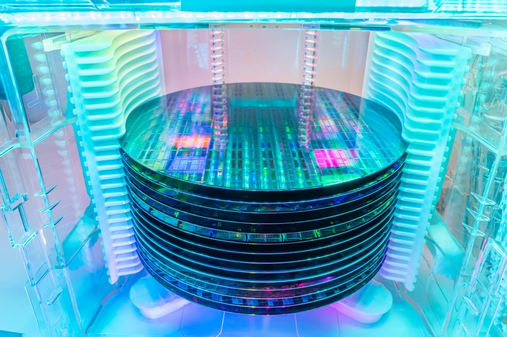
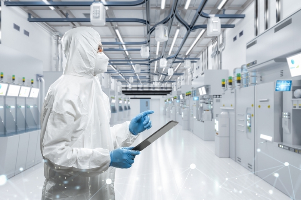
When fully operational, ESMC is expected to have a monthly production capacity of 40,000 300mm (12-inch) wafers on TSMC’s 28/22 nanometer planar CMOS and 16/12 nanometer FinFET process technology, further strengthening Europe’s semiconductor manufacturing ecosystem with advanced FinFET transistor technology. Total investments are expected to exceed 10 billion euros consisting of equity injection, debt borrowing, and strong support from the European Union and German government.
The new facility is expected to generate around 2,000 direct high-tech professional jobs. Additionally, each direct job created by the project is expected to stimulate the creation of numerous indirect jobs throughout the EU supply chain, bolstering the region’s economy. ESMC will uphold TSMC’s standards of sustainability and environmental protection. In line with this mission, ESMC and its partners are dedicated to constructing a green fab that utilizes both existing and cutting-edge techniques to optimize conservation. This includes energy-efficient construction, water reclamation, and obtaining LEED certification.
The establishment of ESMC exemplifies the strength of TSMC’s Grand Alliance, a cornerstone of innovation within the semiconductor industry. This alliance has driven groundbreaking advancements, bringing together TSMC’s partners for a new level of collaboration. The investment in ESMC signifies not just a deeper commitment to this strategic partnership, but also underscores TSMC's unwavering dedication to nurturing innovation across Europe. Construction is expected to start later this year.
“The ESMC wafer fab is to be built right next door to our own Bosch wafer fab in Dresden. So now we will be able to watch it emerge and grow with our own eyes. We’re looking forward to that, just as we are to collaborating closely with our partners TSMC, Infineon, and NXP. Together, we will take Europe a decisive step forward in a key industry, and ensure that advanced chips are available for industrial enterprises here,” said Dr. Stefan Hartung, chairman of the board of management of Robert Bosch GmbH.
"Our joint investment in Dresden once again highlights the enormous significance of Silicon Saxony as a magnet for leading international semiconductor manufacturers," said Infineon Technologies AG CEO Jochen Hanebeck. "The construction of another semiconductor manufacturing facility in Dresden by ESMC constitutes a major success for the region. We are bringing to Europe a particularly important semiconductor technology which is used in the most modern digital chips. This investment will create additional jobs and will permanently strengthen the semiconductor ecosystem in Silicon Saxony, in Germany and in Europe as a whole."
“Today marks a historic milestone for the German and European microelectronics industry,” said NXP President and CEO Kurt Sievers. “NXP is proud to be part of the ESMC joint venture, which will deliver innovative semiconductor solutions and manufacturing capacity focused on Europe’s key markets: the automation and electrification of the automotive and industrial sectors. Today’s groundbreaking ceremony in Dresden on TSMC’s first manufacturing facility in Europe is a significant and tangible step forward for European digital sovereignty.”


