Powering progress: sustainability initiatives driving change in the semiconductor industry

As the global demand for electronic devices, artificial intelligence, machine learning, and high-performance computing continues to surge, the semiconductor industry faces escalating pressure to address its carbon footprint. Although semiconductor companies are making sustainability commitments, more action is needed to achieve net zero.
By Jim Straus, Vice President of Sales and Service, ACM Research
The environmental cost of semiconductor manufacturing is becoming increasingly problematic as the need for advanced technology accelerates. The energy demand is rising as chip design grows more intricate, with semiconductor fabrication facilities operating as some of the most energy-intensive facilities in the world.
Decarbonization efforts also serve as another driver for chip production. Semiconductors are a key component of green technologies such as renewable energy and electric vehicles, facilitating the transition toward a greener economy. On average, electric cars contain about 2,000 chips, roughly double the number of chips in a non-electric car. The number of power semiconductors used in the global renewable energy market is expected to grow with a compound annual growth rate of 8% to 10% from now through 2027.
Many end customers are also putting pressure on suppliers, including semiconductor companies, to step up their efforts to reduce greenhouse gas emissions to achieve net-zero carbon emissions along their entire supply chain. Suppliers and stakeholders are taking heed of these requests, voicing and prioritizing sustainability to accelerate the transition toward a more environmentally responsible future.
To find key strategies and innovations that will drive positive change, companies within the semiconductor industry are pursuing innovative sustainability initiatives to help reshape the landscape of semiconductor manufacturing. From resource-efficient production processes to the development of eco-friendly materials, the semiconductor sector is embracing sustainability as a core principle for future growth.
Closely engaging with customers on developing and refining process technologies that promote the three R’s—reduce, reuse, and recycle – is critical to advancing the industry’s next-zero trajectory. ACM Research embraces this shift toward more environmentally friendly manufacturing processes and facilities by incorporating chemical reduction, defect reduction, and yield improvement into its proprietary technologies.
Reduction of sulfuric acid and hydrogen peroxide mixture
(SPM) usage and raw materials management
Many of the chemicals involved in the production of
semiconductors are hazardous and have environmental implications if not handled
and disposed of properly. Managing the procurement, storage, and safe disposal
of these chemicals adds to the complexity and cost of the manufacturing
process.
To help customers reach sustainability goals, leading semiconductor chipmakers have embraced the circular economy concept, which focuses on reducing, recycling, and reusing materials in a closed loop. With chip production requiring many scarce natural resources, the reduction or reuse of chemicals and materials can significantly decrease its environmental impact. Companies are setting ambitious sustainability goals with the aim of improving waste-management practices and lowering CO2 emissions through product usage. Efforts to reduce CO2 emissions extend to semiconductor fabrication and beyond.
For example, ACM Research promotes the reduction of SPM usage with cutting-edge cleaning systems. Sulfuric acid, mixed with peroxide, is used primarily for the removal of organic materials, such as photoresist. It is considered one of the most widely used chemicals in semiconductor manufacturing and largely impacts the cost of manufacturing/production and the environment. The global electronic-grade sulfuric acid market is projected to reach $415 million by 2026.
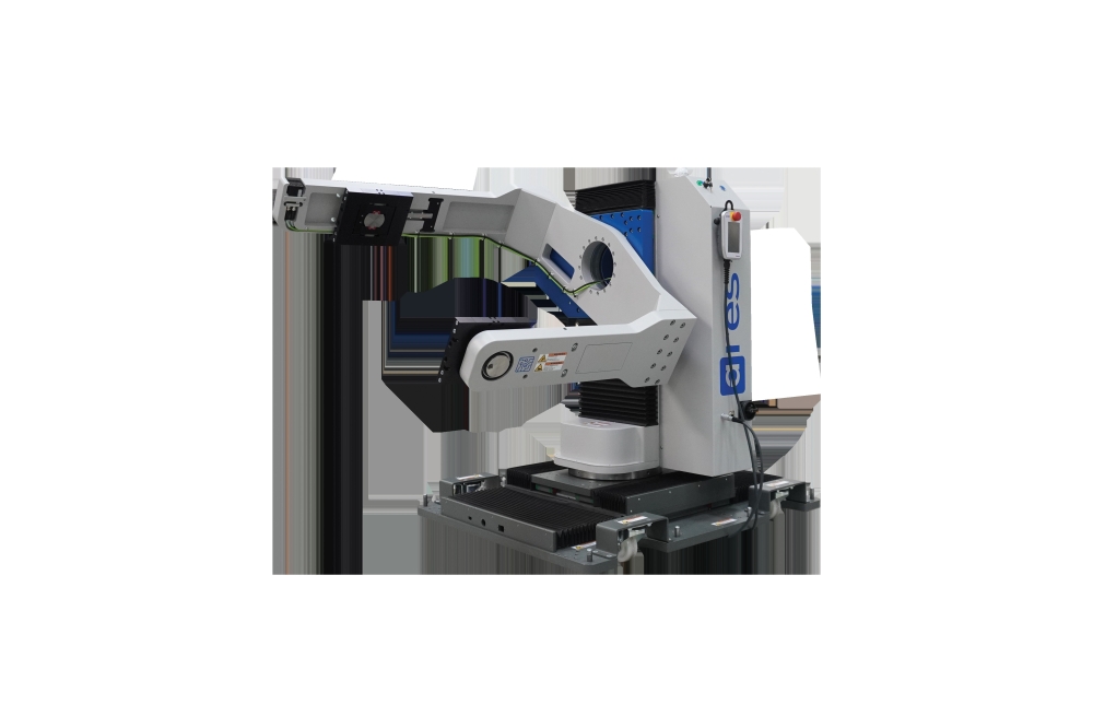
ACM Research’s Ultra C Tahoe cleaning system implements a two-step approach to optimizing the advantages of wet-bench and single-wafer cleaning, thereby reducing energy usage and minimizing waste. About 80% of the sulfuric acid can be reduced, leading to approximately $12 million saved in sulfuric acid usage annually for a 100K wafer production line. Other strategies to consider for handling raw materials involve collaborating with suppliers to source materials with lower emissions, promoting sustainable mining and extraction practices for essential materials like rare-earth elements, and streamlining supply chain logistics to reduce transportation-related emissions.
Water conservation and energy efficiency
During chip production, several million gallons of water are
consumed daily, including ultrapure water (UPW) for multiple cleaning steps,
cooling, and other applications. During chip production, water is used to rinse
and clean silicon wafers, removing debris left from the manufacturing process.
This operation requires UPW, which is thousands of times more pure than
drinking water. It takes roughly 1,400 to 1,600 liters of municipal water to
make 1,000 liters of UPW.
Water conservation and recycling have become necessary to avoid any interruptions in production. Water strategies typically target conservation and reclamation and may include investing in local water treatment.
Chip production at 28nm technology node requires nearly 6 liters of water per square centimeter of wafer, but in the advanced technology node (e.g., nanosheet levels), this figure rises to more than 14 liters. About 75% of the water in a semiconductor fab is used in the manufacturing process, primarily in chemical mechanical planarization and wet clean and etch.
Companies like ACM Research reduces its chemical usage through its H2 functional water and SAPS Megasonix technology. These efforts help protect valuable water resources through effective water usage and reduced processing time. The SAPS Megasonix cleaning technology initiates the formation of H radicals from H2 functional water (dissolved H2 gas bubble), generates surface passivation, and leads to better particle-removal efficiency with reduced deionized water usage.
Energy-efficient semiconductor manufacturing can manifest in a multitude of ways, such as implementing energy-efficient manufacturing processes and technologies, optimizing equipment and machinery to minimize their energy consumption, utilizing advanced cooling systems to reduce energy-intensive heat dissipation, and investing in renewable energy sources, such as solar or wind, to power manufacturing facilities.
By developing semiconductor technologies that rely on lower power consumption, customers can create energy-efficient chips and devices that consume less electricity during use. Implementing product design strategies that prolong the lifespan of semiconductor devices also reduces the need for replacements. The recycling and reuse of semiconductor components and materials encourages long-term resilience.
Advancing customer sustainability goals and initiatives
Manufacturers and suppliers dedicated to helping customers
achieve sustainability goals and reach their zero-waste-to-landfill goals can
do so with tools and technologies designed to reduce, reuse, and recycle the
chemistries used in wafer processing.
As the semiconductor industry continues to play a pivotal role in powering the digital revolution, it is imperative that stakeholders prioritize sustainability to mitigate environmental impacts. Overall, sustainability is becoming a driving force in the semiconductor industry, with companies actively pursuing eco-friendly practices and solutions to reduce their carbon footprint.
The manufacturing chain for semiconductors is remarkably complex and relies on hundreds of different participants. A cohesive and collaborative approach to responsible environmental sustainability relies on efforts by suppliers, manufacturers, end-users, and regulators advocating for a fundamental change in the industry.


