
Biden-Harris Administration reveals preliminary terms with HP
The Biden-Harris Administration has announced that the Department of Commerce and HP Inc. have signed a non-binding preliminary memorandum of terms (PMT) to provide up to $50 million in proposed direct funding under the CHIPS and Science Act.
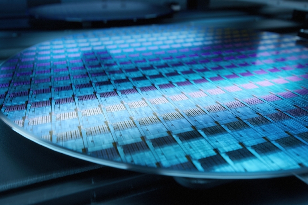
The proposed funding would support the expansion and modernization of HP’s existing facility in Corvallis, Oregon, which is part of the company’s “lab-to-fab” ecosystem in the region that spans from research and development (“R&D”) activities to commercial manufacturing operations. President Biden and Vice President Harris championed the CHIPS and Science Act, a key component of the Investing in America agenda, to usher in a new era of semiconductor manufacturing in the United States, bringing with it a revitalized domestic supply chain, good-paying jobs, and investments in the industries of the future. Through this proposed investment, the Biden-Harris Administration would enhance U.S. technological leadership by driving innovation of groundbreaking semiconductor technologies that serve important end markets, notably including life sciences instrumentation and technology hardware used in artificial intelligence applications.
Rooted in HP’s unique expertise in microfluidics and microelectromechanical systems (“MEMS”), the company’s innovative technology provides a unique pathway to drive improved performance and efficiency of semiconductor-based hardware. Among other products, the proposed funding would support the manufacturing of silicon devices that are key components of life sciences lab equipment which are used in drug discovery, single-cell research, and cell line development. By leveraging HP’s capabilities in microfluidics and MEMS, these devices allow for increased speed and precision during life sciences R&D. The company’s devices serve important focus areas for public health initiatives, and enable performance efficiencies for partner institutions across academia, government, and the private sector including Harvard Medical School, the Centers for Disease Control and Prevention, and Merck.
“The Biden-Harris Administration’s proposed investment in HP shows how we are investing in every part of the semiconductor supply chain and how important semiconductor technology is to innovation in drug discovery and critical life science equipment,” said U.S. Secretary of Commerce Gina Raimondo. “Thanks to President Biden and Vice President Harris’s leadership, the United States will continue leading the world in innovative breakthroughs which all require advanced semiconductor technology while also generating economic opportunity.”
“The Biden-Harris administration continues to deliver on our promise to bring a strong semiconductor ecosystem back to the United States and create good-paying jobs as seen by today’s investment. America invented the chip, and our nation’s ingenuity has always driven us forward,” said Natalie Quillian, White House Deputy Chief of Staff. “HP has long been a part of this great history of American innovation, and thanks to President Biden’s CHIPS and Science Act, we are ensuring that America continues to lead the next generation of technologies.”
The proposed project would build on the company’s 47-year presence in Corvallis and commitment to the local workforce – specifically, the project is estimated to create nearly 150 construction jobs and over 100 manufacturing jobs. The company’s construction partner, Andersen Construction, has entered into a Project Labor Agreement (PLA) for this project. HP plays a pivotal role in the National Science Foundation Engines Development Program–Advancing Semiconductor Technologies in the Northwest to grow the semiconductor industry through strategic opportunities in innovation, entrepreneurship, research, manufacturing, workforce training, and more. Further, HP is working with Portland Community College on training and recruitment programs and has representatives currently serving on a technical advisory council for Linn-Benton Community College. HP has also voluntarily adopted the CHIPS Women in Construction Framework and will work with contractors, trade unions, and other community and workforce partners to implement best practices aimed at expanding the construction workforce by increasing the participation of women and economically disadvantaged individuals.
“It is imperative that we continue to curate and grow a U.S. semiconductor ecosystem where fabs are receiving the latest technology onshore, and then bringing those innovations to market. This all happens with proposed investments in companies like HP,” said Under Secretary of Commerce for Standards and Technology and National Institute of Standards and Technology Director Laurie E. Locascio. “The opportunity that companies such as HP have to push our industry further than we’ve ever gone before is inspiring, motivating and an incredible moment to be a part of. This is all possible thanks to President Biden and Vice President Harris’s CHIPS and Science Act, which is helping position the United States as a global leader for efficiently bringing chips from idea to market and permanently revolutionizing our manufacturing capabilities.”
“This proposed investment provides HP with an opportunity to modernize and expand our facility to further invest in our microfluidics technology, which is the study of the behavior and control of fluid on a microscopic scale. Microfluidics has the potential to drive revolutionary changes across industries, delivering speed, efficiency, and precision, to help pave the way for the next generation of innovation in life sciences and technology. We would like to thank the Biden-Harris Administration and Secretary Raimondo for this proposed investment, as well as the Oregon congressional delegation and state leader for their support and advocacy throughout this process. We look forward to continuing to work to accelerate our innovation in microfluidics and MEMS technology while expanding our manufacturing and R&D capabilities in Corvallis, all made possible by President Biden and Vice President Harris’s CHIPS and Science Act,” said Enrique Lores, President and CEO, HP.
The development and expansion facilitated by the proposed funding would bolster the lab-to-fab ecosystem that HP has established in Corvallis, which also serves as one of three R&D Centers for Excellence within the company’s global footprint. In addition to continued domestic investment in the company’s internal research and development, HP has opened its Corvallis campus to collaborative R&D efforts with academic institutions and startups. Of note, HP donated a 25-year lease of a portion of its Corvallis campus to Oregon State University (OSU) – this 80,000 sq. ft. manufacturing and R&D facility has incubated 39 different companies, including 20 that spun out from OSU faculty and students. The Corvallis campus provides resources and tools for startups and entrepreneurs to build innovative products locally in Oregon and provides an opportunity for these companies to grow and reinvest in the domestic ecosystem.
Additionally, HP aims to use 100% renewable electricity to power its global operations by 2025. The company has indicated that it plans to claim the Department of the Treasury’s Investment Tax Credit, which is expected to be up to 25% of qualified capital expenditures.
As explained in its first Notice of Funding Opportunity, the Department of Commerce may offer applicants a PMT on a non-binding basis after satisfactory completion of the merit review of a full application. The PMT outlines key terms for a potential CHIPS incentives award, including the amount and form of the award. The award amounts are subject to due diligence and negotiation of award documents and are conditional on the achievement of certain milestones. After a PMT is signed, the Department of Commerce begins a comprehensive due diligence process on the proposed projects and continues negotiating or refining certain terms with the applicant. The terms contained in any final award documents may differ from the terms of the PMT being announced today.


