
Electroninks launches Copper MOD Ink
New copper ink displaces electroless copper plating and other industry-standard manufacturing processes with significantly faster production speed, lower ownership cost, and greater sustainability levels.
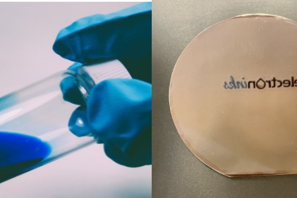
Electroninks has launched the company’s advanced conductive copper ink line. The new copper ink extends Electroninks’ global-leading portfolio of metal complex inks while providing further manufacturing flexibility and lower total ownership costs to customers. Electroninks will be showcasing the new copper ink line at booth Q5152 in Hall 1 of SEMICON Taiwan September 4-6, 2024.
A high-demand application for the new copper ink is seed layer printing for fine-line metallization and RDL formation in combination with the company’s proprietary iSAP™ process. For this application, Electroninks copper ink effectively displaces industry use of electroless (e-less) copper plating and physical vapor deposition (PVD) tie layers while achieving a significant increase in manufacturing throughput and a vast reduction in ESG footprint. Compared to legacy methods (PVD and e-less), ink-based additive printing uses a fraction of the water and energy, factory footprint and CAPEX, thus providing customers with the lowest total cost of ownership and highest ROI on the market.
The copper inks are deposited by spray coating, screen printing, inkjet, spin-on, and other conventional printing methods. Beyond the seed layer application, Electroninks is working with customers on a multitude of applications, including advanced packaging, serving a diversity of markets. “These copper inks bolster Electroninks’ strong and diverse MOD ink product portfolio and deliver best-in-class ESG and cost savings to customers.” stated Brett Walker, CEO and co-founder of Electroninks.
“MOD inks, which have been on the market from Electroninks for a few years now, provide unique properties that are well suited for today’s semiconductor wafer and module-based packages requiring high performance thermal and power management.” stated Jim Haley, Vice President of Marketing, IMAPS Executive Council. “By introducing a copper-based MOD product, markets and customers are generally more supportive, as copper is a standard in electronic design for many use-cases. While silver, gold, and other MOD inks will continue to serve this market, we welcome copper MOD inks to address key needs in advanced packaging.”
Electroninks is offering a range of copper ink grades to address customer demand for adhesion to various substrates, including glass, silicon, and EMC. These inks are compatible with multiple printing techniques and can be cured at low temperatures for short times – as low as 140C in 5 minutes under nitrogen or ambient conditions.


