ATE testing challenges of heterogeneous silicon chips with advanced packaging

The semiconductor industry is rapidly evolving, driven by the increasing demand for more powerful, efficient, and versatile devices. This evolution has led to the development of complex heterogeneous semiconductor chips with ultra-high density and advanced silicon packages. These cutting-edge designs integrate various functionalities, materials, and technologies onto a single chip, making them incredibly powerful but also posing significant testing challenges in the manufacturing flow.
By Sriharsha Vinjamury, Principal Engineer, SOPT, ARM Inc
The push for heterogeneity in silicon packages is aimed at enhancing computational performance, energy efficiency, and system adaptability. By integrating various types of processors—such as CPUs, GPUs, FPGAs, and AI accelerators—these packages can optimize task execution. Heterogeneous integration enables specific processors to handle workloads they are architecturally optimized for, resulting in significant energy savings and performance boosts. Additionally, it facilitates system upgrades and customization, allowing new functionalities to be added without necessitating a complete system redesign. Enhanced thermal management techniques distribute the computational load more evenly, maintaining lower operating temperatures and improving component reliability.
This approach drives innovation, enabling bespoke solutions for applications ranging from hyperscale data centers to portable consumer electronics. Furthermore, it is cost-effective, extending the operational lifespan of technology and minimizing the frequency and cost of updates.
Silicon Performance improvements with heterogeneous Integration.
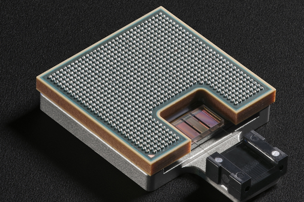
A heterogeneous package with 3D HBM memory stacking and an AI accelerator chip
Challenges faced in Advanced Packages:
One of the primary issues in advanced packaging is material compatibility and selection. Ensuring strong adhesion between diverse materials such as organic substrates, silicon dies, and metal interconnects is critical. Poor adhesion can lead to delamination, impacting device reliability. Additionally, different materials have varying coefficients of thermal expansion (CTE), which can cause mechanical stress during thermal cycling, potentially resulting in cracks or warpage.
Lithography and patterning also pose significant challenges. Achieving precise patterning for redistribution layers (RDLs) and interconnects at sub-micron scales is difficult. Variations in these processes can cause electrical performance issues and reduce yield. Accurate alignment between multiple layers in multi-die or 3D ICs is crucial, as misalignment can result in connectivity failures and diminished performance.
The nano-scale lithography for the RDL layers pose issues for reduced line widths, requiring precise electromigration control. Integrating low-k dielectrics and novel metals demands strong adhesion and diffusion barriers. Efficient thermal management and stress-relief structures are crucial for differential CTE-induced stress. Maintaining high-frequency signal integrity and controlling defects in photolithography, etching, and plating are essential for yield and reliability in complex, high-density interconnects.
A Heterogeneous Package with 3D HBM memory stacking and an AI accelerator chip.
Thin wafer handling is nothera major challenge in advanced packaging because thinning wafers to just a few hundred micrometers for 3D stacking makes them fragile and prone to breakage and warpage, necessitating special handling during processing. Through-silicon vias (TSVs) add another layer of difficulty with their complex etching and filling processes; defects here can seriously compromise performance and reliability. Additionally, TSVs can introduce stress that degrades silicon performance over time, especially under thermal cycling.
Thermal management is crucial as high-density interconnects and multiple dies generate significant heat, which needs to be efficiently dissipated to prevent overheating. This requires appropriate thermal interface materials (TIMs). Ensuring interconnect reliability is also tough, as high current densities can lead to electromigration, causing connection failures. Repeated thermal cycling adds stress that can crack interconnects over time.
In assembly and bonding, achieving reliable flip-chip bonding with micro-bumps demands precise control over bump formation, alignment, and reflow. Optimizing the underfill process is critical to protect solder joints from environmental stresses.
Managing yield and defects throughout the stages of lithography, etching, and bonding is vital, as any defects can significantly affect production efficiency. Environmental concerns like moisture sensitivity and outgassing must be managed to ensure long-term reliability. Finally, balancing cost and scalability is essential. Advanced packaging processes are inherently complex and expensive, requiring constant innovation and collaboration to maintain high yield and commercial viability.
These issues impact yield and introduce latent defects. Variations in these processes can lead to electrical performance issues, misalignments, and stress-induced failures, which are difficult to detect during Automated Test Equipment (ATE) testing. Defects like delamination, warpage, and electromigration often manifest under operational stresses, making early detection and effective fault isolation challenging, ultimately affecting the overall reliability and yield of the devices.
Mechanical failure in RDL, source AMKOR.
ATE testing overview
Automated Test Equipment (ATE) plays a pivotal role in evaluating large samples and is essential for the production testing of newly fabricated silicon chips. As a cornerstone of semiconductor manufacturing, ATE’s primary job is to offer an automated, cost-effective testing solution that boosts device throughput significantly. By automating the testing process, ATE not only slashes the time and costs linked with manual testing but also enhances the accuracy and reliability of these tests. When combined with System-Level Testing (SLT), ATE creates a robust testing framework that supports the mass production of chips while upholding high quality standards.
ATE testing NPI and Production Flow.
Types of Tests Conducted by ATE
Structural Testing:
• Purpose: Identify manufacturing defects in silicon chips.
• How It Works: DFT engineers use fault modeling to create test patterns for various faults.
• Examples: ATPG for Stuck-At Faults (SAF), Transition Delay Fault (TDF), Boundary-Scan Description Language (BSDL)/Boundary Scan (BSCAN), Logic Built-In Self-Test (LBIST).
Functional testing:
• Purpose: Ensure the electronic device operates according to specifications.
• Examples: Testing a microcontroller to verify data processing and signal generation.
Parametric testing:
Purpose: Measure specific electrical parameters like voltage, current, and resistance.
Example: Checking power supply voltage levels within the specified range.
Integration flow: Tests are combined into a flow influenced by factors like wafer stage or final test stage, temperature conditions, and board complexity.
Additional testing for system-level performance and reliability:
• System-Level testing (SLT): Evaluate overall system performance.
• Stress testing: Assess robustness under extreme conditions.
• Burn-In testing: Identify early-life failures by running devices at elevated temperatures.
• Environmental testing: Evaluate performance under various conditions like humidity, temperature, and vibration.
Key phases in Device Bring-up on ATE
The Bring-Up or New Product Introduction (NPI) phase is the initial but the most crucial stage in the lifecycle of Automated Test Equipment (ATE) operations, crucial for accurate and efficient testing of newly developed semiconductor devices before mass production. Key activities include system configuration and setup, test program development, debugging and validation across platforms, Internal part distributions, Providing Engineering and Customer Samples to the End customer and finally, flow optimization and production release. The Production Phase is the second and ongoing stage in ATE operations, focusing on high-volume testing and continuous improvement to ensure consistent high-quality and efficient manufacturing. Key activities include high-volume testing, ongoing calibration and maintenance, yield monitoring and improvement, test program updates, cost reduction and efficiency enhancements, and quality assurance and reliability testing.
Key process parameters are meticulously tracked at various stages and fed back to the fabs. The fabs provide Wafer Acceptance Test (WAT) parameters, allowing us to compare these metrics against design targets and make informed decisions. Given that Automated Test Equipment (ATE) operates in a volume-driven environment, advanced data analysis tools are essential for identifying systematic and random process-related patterns on the wafers. However, these issues can be latent, only manifesting during later stages of device aging. Detecting such latent defects during the testing phase is challenging, as it requires sophisticated fault isolation techniques and predictive analytics to ensure long-term chip reliability.
ATE ramp-up timelines based on defect density.
Challenges and recommendations faced in testing advanced packages
A single multi-die configuration constitutes different special-purpose components including CPUs, GPUs, memory arrays, analog/RF circuits, specialized accelerators, and so on. This increased complexity increases the functional verification and debugging requirements. The traditional methodologies developed for 2D testing are more likely to be inadequate and thus call for advanced techniques like hierarchical test methodologies and advanced Design-for-Testability architectures to increase Fault coverage and observability.
Low accessibility to deeper nodes
The vertical and horizontal integration of different dies in a heterogeneous package makes the access of internal nodes difficult for proper testing and debugging. The access mechanisms for all those nodes, without disturbing the functionality of the device, come through innovative solutions such as boundary scan testing, advanced BIST circuits, and micro-probing technologies. These techniques have enabled non-intrusive monitoring and diagnosis of embedded components with very little degradation of device performance.
Advanced ATPG algorithms, such as dynamic compaction, X-filling, and fault simulation, enhance test efficiency by generating highly compact test patterns, reducing test time, and improving fault coverage. Techniques like SAT-based ATPG leverage satisfiability solvers for complex fault detection, ensuring robust testing of intricate semiconductor designs. These methods address challenges in heterogeneous packages, ensuring high reliability and performance
Heat dissipation
The larger the number of high-performance active components that are integrated into heterogeneous packages, the greater the thermal management problems are. Advanced methods of heat dissipation shall be needed with thermal vias, microfluidic channels, and high conductivity TIMs. Efficient management of heat transfer minimizes thermal hotspots and ensures a constant distribution of temperature that does not result in thermal-induced performance degradation or device failure.
Thermal profiling
The bring-up phase itself is a critical part of discovering and mitigating potential thermal issues. Sophisticated thermal simulation tools such as Computational Fluid Dynamics and Finite Element Analysis are further combined with infrared thermal imaging to provide valuable details of thermal
maps. These help in designing an effective cooling solution and instructing on where the die should be placed and what kind of materials to use for packaging.
Power delivery network design
It should ensure that there is stable and efficient power delivery with minimal IR drop and noise and power integrity issues for all the integrated components in heterogeneous packages. Advanced materials with superior electrical properties, on-die decoupling capacitors, and hierarchical schemes of power distribution could be applied to avoid higher current densities and intrinsic reduced noise margins in more densely integrated structures.
Advanced board designs
Designing advanced boards for next-gen silicon packages faces challenges like achieving ultra-high routing density with micro-vias and buried vias, maintaining signal integrity with controlled impedance traces, differential pair routing, and
low-loss dielectrics, and ensuring power integrity with dedicated power/ground planes and decoupling networks. Effective thermal
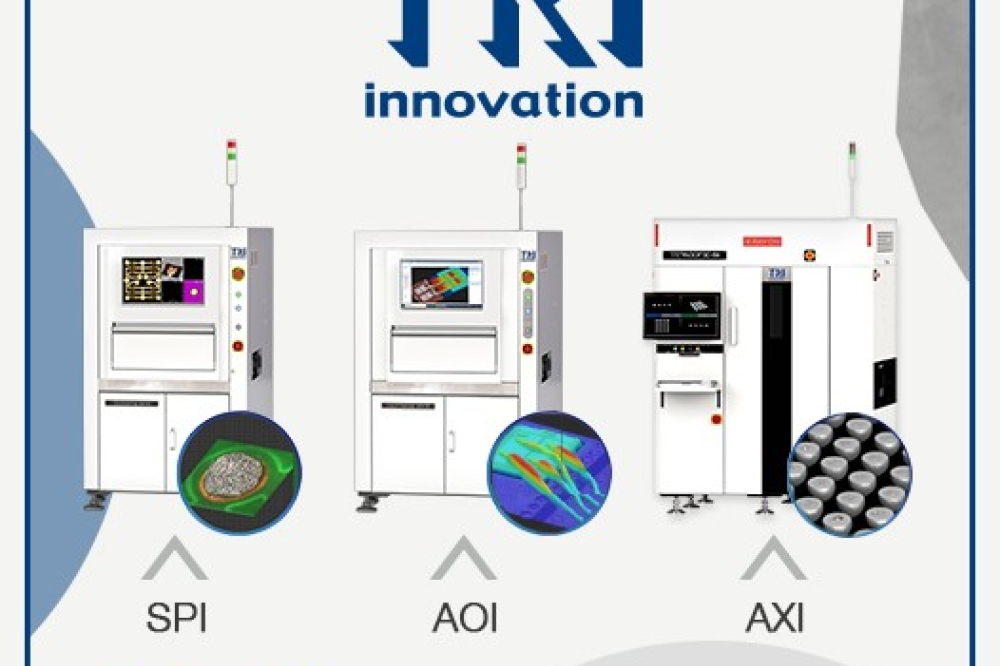
management requires integrated heat spreaders, thermal vias, pads, and metal-core PCBs. Precision manufacturing tolerances and enhanced inspection techniques like AOI and X-ray are essential for reliability.
High-speed design features such as via-in-pad technology and backdrilling reduce parasitic effects, while embedded/co-packaged components improve performance. Advanced simulation
tools for electromagnetic and thermal analysis optimize the design, and test sockets facilitate robust and repeatable testing of high-performance devices.
Defect density during production testing
Compared with traditional 2D chips, heterogeneous packages may involve more process-induced defect density because of an increased number of fabrication steps, additional die-to-die bonding, and more inter-component connections. Advanced defect inspection techniques, like e-beam inspection or AOI, must be combined with SPC for detecting defects and reducing them to improve yield rates.
Time-to-market challenges
High defect density in advanced silicon packages delays device bring-up and extends development timelines. Complex testing and debugging, including advanced ATPG, DDR, and high-speed I/O (HSIO) bring-up, require sophisticated protocols and extensive validation, significantly prolonging the process. Efficient thermal management and signal integrity maintenance demand detailed analysis and optimization, adding to development time.
Debugging intricate issues, such as timing violations and cross-talk in HSIO, can be time-consuming, further delaying deliverables. Power integrity challenges and ensuring robust manufacturing tolerances also contribute to extended timelines.
Inter-component reliability
To ensure the reliability of interconnections in heterogeneous packages, implement self-healing interconnects using conductive polymers or nano-composites that autonomously repair minor cracks. Utilize AI-driven predictive maintenance by analyzing real-time data from embedded sensors to anticipate and prevent failures. Integrate quantum dot-based stress sensors within interconnects for highly sensitive, real-time monitoring of stress and temperature. Develop adaptive thermal management systems that dynamically adjust cooling strategies using phase-change materials and microfluidic channels based on real-time thermal profiling. Employ advanced nanomaterials like graphene to create interconnects with superior electrical, thermal, and mechanical properties, significantly enhancing durability and performance under extreme conditions.
Cost effectiveness
The complex fabrication process and reduced yields at the start for heterogeneous packages can make them more expensive to produce. In order to have an economic package, balancing production costs against the market requirements includes enhancing the fabrication process, introducing lower cost-effective materials, and economies of scale. However, the Performance benefits Heterogenous integration offers precedes the cost of producing these chips.
Cost versus performance between 2D monolithic and Heterogenous packages.
Scalability
Increased demand for heterogeneous packages makes scalability an essential criterion. This means developing manufacturing techniques to be scaled up, like advanced lithography methods, wafer-level packaging, and automated assembly lines, so large-scale production can be attained without sacrificing quality or yield, answering the demand of the market. Increased demand for heterogeneous packages makes scalability an essential criterion. This means developing manufacturing techniques to be scaled up, like advanced lithography methods, wafer-level packaging, and automated assembly lines, so large-scale production can be attained without sacrificing quality or yield, answering the demand of the market.
Conclusion
The evolution of heterogeneous silicon chips with advanced packaging presents both significant challenges and unparalleled opportunities.
Addressing issues such as high defect density, complex thermal management, and ensuring inter-component reliability requires innovative solutions like advanced ATPG algorithms, AI-driven predictive maintenance, and self-healing interconnects.
While the initial cost and complexity of producing these advanced packages are higher, the substantial performance improvements and long-term benefits justify the investment. By leveraging cutting-edge technologies and methodologies, the semiconductor industry can achieve scalable, high-yield production, meeting the growing demand for more powerful, efficient, and adaptable devices.
Ultimately, these advancements will drive the next wave of innovation in fields ranging from data centers to consumer electronics, paving the way for a future where technology continues to evolve at an unprecedented pace.
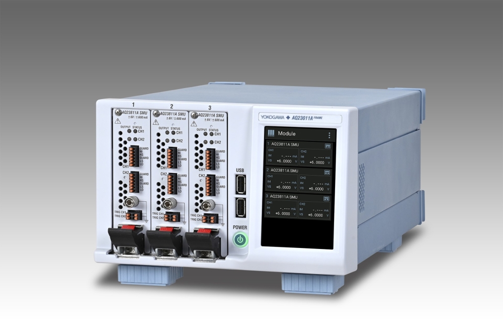
A Generic ATE test system.


