
ACM Research expands Fan-Out Panel-Level Packaging portfolio
New double-sided bevel etching system enhances process efficiency and reliability in copper-related applications, supporting high-precision features on large panels.
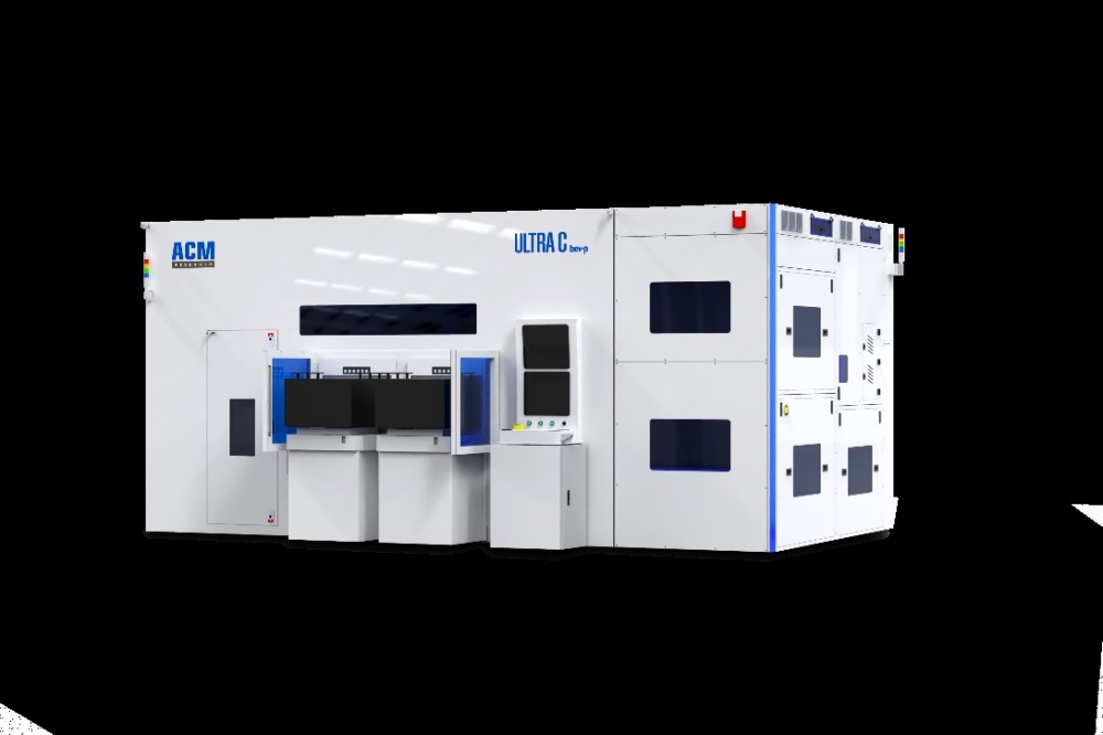
ACM Research has launched its Ultra C bev-p panel bevel etching tool for fan-out panel-level packaging (FOPLP) applications. The new tool is specifically designed for bevel etching and cleaning in copper-related processes and is capable of handling both the front and back sides of panel bevel etching within a single system. This capability enhances process efficiency and product reliability.
“We believe FOPLP will gain prominence as it meets the evolving demands of modern electronic applications, offering advantages in integration density, cost efficiency and design flexibility,” said Dr. David Wang, ACM’s president and chief executive officer. “Our new Ultra C bev-p tool leverages ACM's deep expertise in wet processing to deliver what we consider to be advanced performance, and we believe it is one of the first tools to employ double-sided bevel etching for horizontal panel applications. We expect the Ultra C bev-p, alongside our recently announced Ultra ECP ap-p for horizontal panel electrochemical plating and Ultra C vac-p flux cleaning tools, to bolster the FOPLP market by facilitating advanced packaging on large panels with high-precision features.”
The Ultra C bev-p tool is a key enabler for FOPLP processes, utilizing a wet etching technique designed specifically for bevel etching and copper residue removal. This process is crucial for preventing electrical shorts, minimizing contamination risks, and maintaining the integrity of subsequent processing steps, ensuring the long-term reliability of devices. At the core of the tool’s effectiveness is ACM’s patented technology that addresses the unique challenges posed by square panel substrates.
Unlike traditional round wafers, ACM’s innovative design ensures a precise bevel removal process that remains confined to the bevel region, even on warped panels. This advancement is vital for maintaining the integrity of the etching process and achieving the high performance and reliability required by advanced semiconductor technologies.
Key Features
The Ultra C bev-p tool is designed specifically for panel substrates, offering compatibility with organic, glass, and bonding panels. It efficiently manages both the front and back sides of panels, accommodating sizes from 510 mm x 515 mm to 600 mm x 600 mm, with thicknesses ranging from 0.5 mm to 3 mm. The tool can handle warpages up to 10 mm, ensuring optimal processing conditions.
Advanced Panel Handling: Equipped with a single robot for secure and precise panel handling and transfer.
Efficient Copper Removal: Utilizes diluted sulfuric acid and peroxide (DSP) — a mixture of deionized (DI) water, sulfuric acid, and hydrogen peroxide — for effective copper removal. It also includes DI water for rinsing and N2 for final drying, ensuring a clean and dry surface.
High Throughput: Capable of operating up to six processing chambers, the Ultra C bev-p achieves a throughput of 40 panels per hour (PPH), making it highly efficient for high-volume production.
The system offers bevel control accuracy of ±0.2 mm and an exclusive control range of 0-20 mm. It is designed with a mean time between failures (MTBF) of 500 hours and an uptime of 95%, ensuring exceptional reliability, consistent performance, and operational efficiency.


