Element Six wins U.S. Department of Defense UWBGS program

Element Six (E6) is leading a program under UWBGS (Ultra-Wide BandGap Semiconductors), an initiative established by the United States Defense Advanced Research Projects Agency (DARPA), to enable the next generation of semiconductor technologies.
Through the UWBGS program, DARPA’s Microsystems Technology Office has stated its goal to develop high-quality ultra-wide bandgap (UWBG) materials, such as substrates, device layers, and junctions. These materials are key to realizing advanced electronics, including high-power RF switches, amplifiers for radar and communications, high-voltage power switches, high-temperature electronics for extreme environments, and deep ultraviolet (UV) LEDs and lasers, underpinning a multi-billion dollar system market.
Diamond offers the potential for superlative semiconductor device performance, lowering overall size, weight and power consumption (SWaP) thanks to outstanding properties such as its chemical and radiation inertness, high carrier mobility, superlative heat conduction, and wide electronic bandgap.
E6’s contribution to the UWBGS programme will harness the company’s expertise in large area CVD polycrystalline diamond and high-quality single crystal (SC) diamond synthesis, to realize 4-inch device grade SC diamond substrates
Prof. Daniel Twitchen, Chief Technologist at Element Six, said: “We are proud to work alongside the other DARPA UWBGS program partners. Industrial diamond has disrupted multiple markets since its first scale synthesis in the 1950s, and I am confident that technology breakthroughs in UWBGS will help unlock another 70 years of opportunities in the semiconductor industry.”
Element Six’s SC diamond was already a crucial enabler in the CERN Large Hadron Collider’s monitoring systems, helping lead to the discovery of the Higgs Boson Particle and, in partnership with high-power semiconductor leader ABB, E6 realized the first high-voltage bulk diamond-based Schottky diodes. Furthermore, E6 recently completed build and commission of an advanced CVD facility, leveraging its core technology in Portland (OR), powered by renewable energy sources.
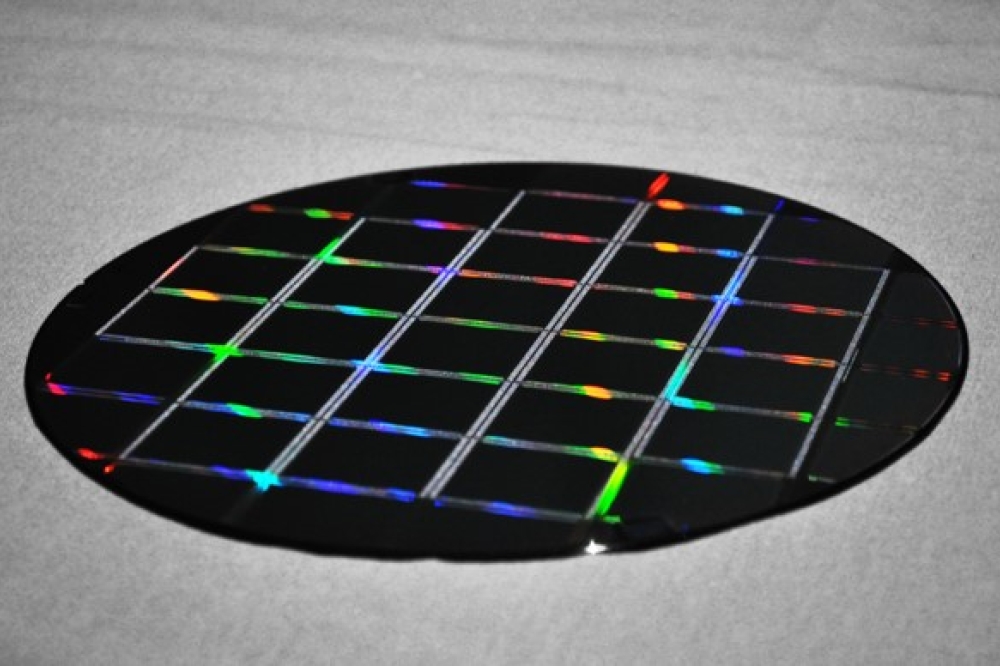
E6 polycrystalline diamond wafers measuring >4 inches are already enabling telecommunication infrastructures and defence applications, being used as either optical windows in EUV lithography for state-of-the-art silicon (Si) chips, or in thermal management applications for high-power density Si and gallium nitride (GaN) semiconductor devices.
For the UWBGS program, Element Six has partnered with other leaders in the field from across the globe: Orbray in Japan (with large-area diamond expertise - full partnership announcement available here), Raytheon (leaders in GaN RF devices), Hiqute Diamond in France (with dislocation engineering expertise), and Stanford and Princeton Universities in the US (with materials bulk and surface processing characterization expertise).
Through the collaboration of this global network of technology leaders, UWBGS will push the boundaries of diamond innovation to enable a new generation of ultra-wide bandgap semiconductors.


