
AEM expands system level test on AMPS Platform
AEM is expanding System Level Test (SLT) capability on its unique test cell platform Asynchronous Modular Parallel Smart (AMPS).
The modular AMPS platform offers solutions from lab and engineering to high-volume manufacturing (HVM) for Burn-In and SLT. The AMPS solution empowers integrated circuit (IC) manufacturers to achieve extensive test coverage in a cost-effective manner and accelerate their time to market.
SLT is conducted at the end of the semiconductor fabrication process, where IC performance is verified in its end-use environment. Due to the increasing IC complexity and chiplet advanced packaging, IC manufacturers are increasing the adoption of SLT to improve product quality and reduce field returns. Key growth areas for SLT are high performance compute (HPC) and artificial intelligence (AI) applications with requirements for higher power beyond 2,000 watts per device.
AEM has been a pioneer in SLT since 2002 and has shipped over 1,000 systems worldwide. The latest AMPS platform offers customers unparalleled flexibility, with a full-stack test interface that includes high-throughput automation, application-specific test instruments, test sockets, and thermal management. Its modular design allows customers to scale from engineering systems with fewer test sites to high-throughput production with hundreds of sites, all equipped with its common thermal pathway - PiXL.
PiXLTM - AEM’s Patented Thermal Engine for Intelligent Multi-zone Control
AMPS features AEM’s advanced active thermal control engine, PiXL. PiXL allows for high-precision and device-specific thermal control to test high-power AI/HPC chips and advanced packages.
AMPS Platform delivers:
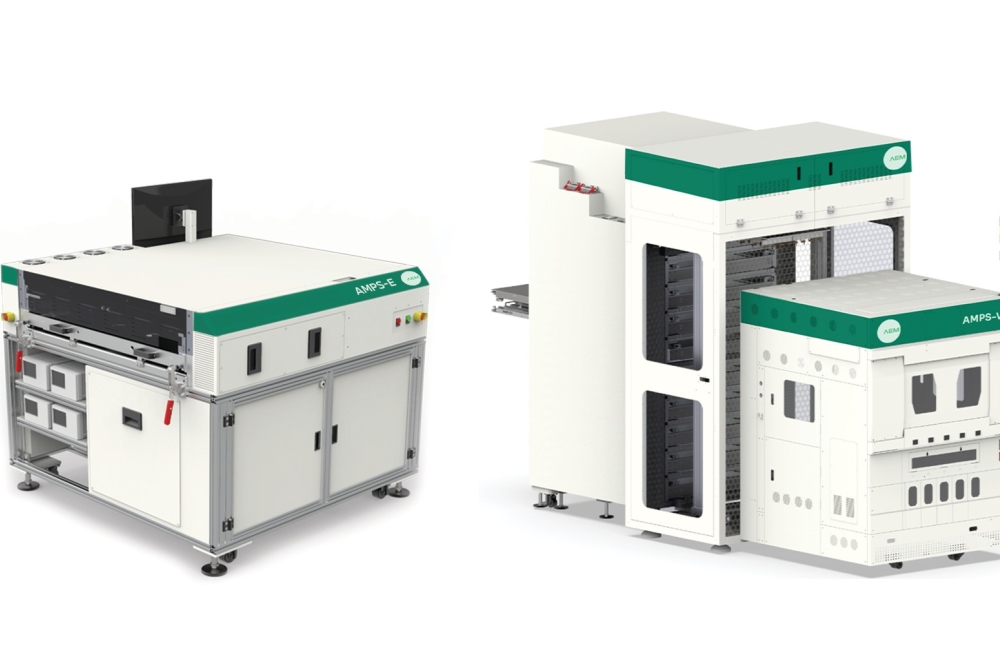
Lab to Manufacturing: The AMPS platform’s modular architecture utilizes the same configurable test unit (CTU) in the lab/engineering configuration (AMPS-E) and HVM configuration (AMPS-V10) — 3D stackable CTU design to optimize floor space.
CTU: Each CTU is fully configurable and supports over 32 sites per CTU. It features the PiXL thermal engine, which can handle over 2kW per device.
Parallelism: AMPS-E supports a single CTU and over 32 sites. AMPS-V10 supports 10 CTUs and over 320 sites.
Device Types: Supports advanced package formats, scalable beyond 100mm x 100mm package sizes.
Factory 4.0 Automation: Fully supports JEDEC-based I/O with full Factory 4.0 automation.
Amy Leong, CEO of AEM, shared, “Our customers are working with advanced packaging, where traditional test methods no longer offer sufficient coverage to guarantee a higher level of quality and reliability, which is critical for their end-users. The modular platform for System Level Test and Burn-in, powered by our PiXL thermal technology, enables our customers to ship their products confidently.”
AEM's Test 2.0 paradigm is at the forefront of test solutions for next-generation advanced logic devices, including high-performance compute and AI. AEM leads the industry in Active Thermal Control, Advanced Factory Automation, and Test Instrumentation.


