Testing time in Taiwan
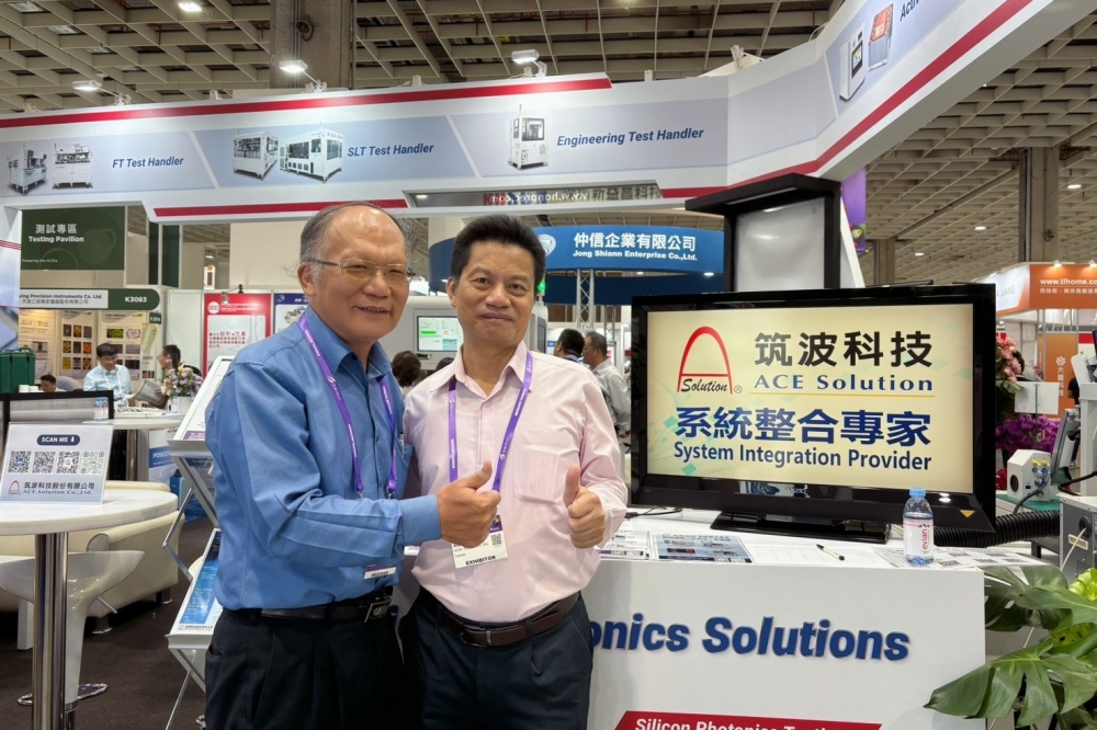
SEMICON Taiwan officially opened on September 6, 2024, with ACE Solution and HON. PRECISION joining forces to showcase latest advancements in silicon photonics testing technology, precision measurement, and automated machinery integration.
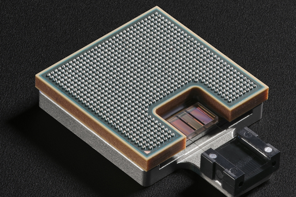
Their exhibition focused on high-density optoelectronic integration testing solutions designed to meet the increasing demands of silicon photonics for high-capacity and high-channel testing. The integrated optoelectronic signal testing system effectively addresses the challenges posed by increased data center traffic and high-speed transmission needs, significantly boosting transmission rates and reducing energy consumption. With semiconductor packaging evolving towards Co-Packaged Optics (CPO), ACE Solution highlighted its silicon photonics solutions developed through deep collaboration with Quantifi, integrating PXI testing modules to offer an efficient, multi-system testing solution supporting 800G and 1.6T high-speed transmission. These integrated solutions meet the research and production needs for high-speed, high-precision, and high-efficiency testing while offering programmable automation for flexible applications.
ACE Solution also demonstrated its latest innovations in compound semiconductor testing. The Teradyne ETS-88 testing platform is widely used for SiC, GaN, PMIC, automotive electronics, aerospace, and defense industries. Key features include multi-site CP, second-contact KGD, dynamic/static power device FT, and fully automated high-output module FT. The ETS-364 and ETS-800 platforms are tailored for mixed-signal, digital, and analog testing, offering the industry's highest-spec power IC testing capabilities with support for up to 6000V and 4000A, making them ideal for high-current, high-voltage applications, particularly in EV power and battery management.
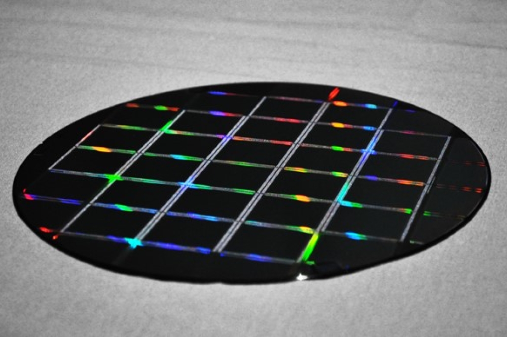
The TZ-6000 non-destructive wafer and materials inspection system utilizes terahertz (THz) technology, focusing on compound semiconductor testing for GaAs, SiC, and GaN. It offers greater penetration depth and flexibility, handling various sizes and shapes of wafers. Equipped with advanced wafer probes and intelligent software analysis, it can simultaneously measure parameters such as thickness, refractive index, resistivity, dielectric constant, surface/subsurface defects, and full wafer scans, enabling non-destructive wafer quality measurements.
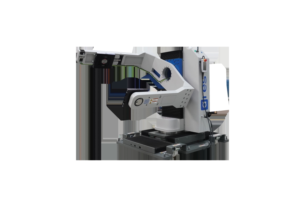
The Electro-Optic Terahertz Pulse Reflectometer (EOTPR) is the world's first instrument to use isolation technology to detect IC package faults and monitor package quality, making it ideal for non-destructive defect detection in 3DIC package analysis. With 5-micron pinpoint precision, the EOTPR is widely used in advanced IC packaging fault analysis for devices such as stacked packages (PoP), flip-chip, and TSV in 3D packaging. Major semiconductor companies have extensively deployed EOTPR for advanced IC packaging quality assurance in manufacturing environments.
Steve Hsu, President of ACE Solution, stated, "With over 20 years of experience in hardware-software integration, ACE Solution has expanded from wireless communication testing to various testing fields, meeting the needs of our local clients. We are thrilled to collaborate with HON. PRECISION to showcase our achievements in automation and precision testing."
Alan Hsieh, President of HON. PRECISION commented, "This exhibition marks a new milestone in our partnership with ACE Solution. We look forward to offering more advanced solutions, fostering greater collaboration and innovation across the industry."


