
An industry game-changer?
Infineon pioneers world’s first 300 mm power gallium nitride (GaN) technology.
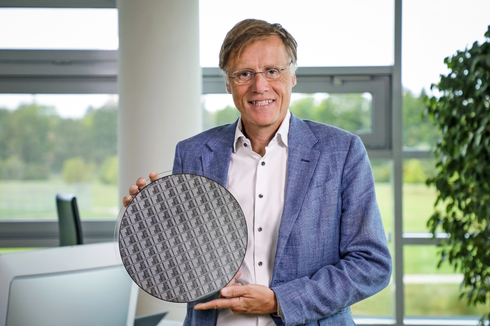
Infineon Technologies has succeeded in developing the world’s first 300 mm power gallium nitride (GaN) wafer technology. Infineon believes that it is the first company in the world to master this groundbreaking technology in an existing and scalable high-volume manufacturing environment. The breakthrough will help substantially drive the market for GaN-based power semiconductors. Chip production on 300 mm wafers is technologically more advanced and significantly more efficient compared to 200 mm wafers, since the bigger wafer diameter offers 2.3 times more chips per wafer.
GaN-based power semiconductors find fast adoption in industrial, automotive, and consumer, computing & communication applications, including power supplies for AI systems, solar inverters, chargers and adapters, and motor-control systems. State-of-the art GaN manufacturing processes lead to improved device performance resulting in benefits in end customers’ applications as it enables efficiency performance, smaller size, lighter weight, and lower overall cost. Furthermore, 300 mm manufacturing ensures superior customer supply stability through scalability.
“This remarkable success is the result of our innovative strength and the dedicated work of our global team to demonstrate our position as the innovation leader in GaN and power systems,” said Jochen Hanebeck, CEO of Infineon Technologies AG. “The technological breakthrough will be an industry game-changer and enable us to unlock the full potential of gallium nitride. Nearly one year after the acquisition of GaN Systems, we are demonstrating again that we are determined to be a leader in the fast-growing GaN market. As a leader in power systems, Infineon is mastering all three relevant materials: silicon, silicon carbide and gallium nitride.”
Infineon has succeeded in manufacturing 300 mm GaN wafers on an integrated pilot line in existing 300 mm silicon production in its power fab in Villach (Austria). The company is leveraging well-established competence in the existing production of 300 mm silicon and 200 mm GaN. Infineon will further scale GaN capacity aligned with market needs. 300 mm GaN manufacturing will put Infineon in a position to shape the growing GaN market which is estimated to reach several billion US-Dollars by the end of the decade.
This pioneering technological success underlines Infineon's position as a global semiconductor leader in power systems and IoT. Infineon is implementing 300 mm GaN to strengthen existing and enabling new solutions and application fields with an increasingly cost-effective value proposition and the ability to address the full range of customer systems. Infineon will present the first 300 mm GaN wafers to the public at the electronica trade show in November 2024 in Munich.
A significant advantage of 300 mm GaN technology is that it can utilize existing 300 mm silicon manufacturing equipment, since gallium nitride and silicon are very similar in manufacturing processes. Infineon’s existing high-volume silicon 300 mm production lines are ideal to pilot reliable GaN technology, allowing accelerated implementation and efficient use of capital. Fully scaled 300 mm GaN production will contribute to GaN cost parity with silicon on R DS(on) level, which means cost parity for comparable Si and GaN products.
300 mm GaN is another milestone in Infineon’s strategic innovation leadership and supports Infineon’s mission of decarbonization and digitalization.


