Optogenetic OLED-on-CMOS stimulators for neurosensory therapies

Researchers from the Fraunhofer Institute for Photonic Microsystems IPMS and the Max Planck Institute for Multidisciplinary Natural Sciences (MPI-NAT) have researched optical stimulators for future cochlear implants as part of the "NeurOpto" project (funded by the Fraunhofer-Max-Planck Cooperation Program: 601001).
They will present tiny OLED-on-silicon-based probes for the first time at W3+ 2024 in Jena, on September 25 and 26, 2024, at booth No. C12.
What is Optogenetics?
Optogenetics is a method that uses light to control genetically modified cells in living tissues. By introducing light-sensitive proteins into cells, their activity can be precisely turned on and off with light pulses. This technique is commonly used in neuroscience to study the functions of nerve cells and to activate or inhibit specific neuronal populations. To deliver light precisely to stimulate tiny cells, small and locally selective light sources are therefore needed now.
Dr. Uwe Vogel, Head of business unit "Microdisplays and Sensors" at Fraunhofer IPMS, explains: "With OLED-on-silicon technology, we can bring tiny, locally controllable light pixels onto a chip. This chip can be flexibly designed to reach the desired locations even in curved structures like the cochlea. This allows light to be used precisely where electrical stimulation alone is insufficient."
Prof. Tobias Moser from MPI-NAT adds: "The development of optical cochlear implants promises better hearing for the severely hearing impaired. MPI-NAT and University Medical Center Göttingen (UMG) are working closely with partners such as Fraunhofer IPMS on the technological solutions required for this. Intelligent implantable stimulators based on optical stimulation could also be used for other medical therapies such as laryngeal pacemakers, cardiac pacemakers, pain relieve, retinal implants, or deep brain stimulation."
How does optical cell stimulation work?
Current electrical cochlear implants (eCIs) restore speech comprehension in quiet environments for most of the approximately 1 million users worldwide. However, speech recognition in background noise and enjoyment of music are often severely limited. The reason for this is the inadequate frequency resolution of electrical sound coding: each electrode contact also stimulates more distant nerve cells that code different frequencies due to the broad current spread. Since light can be controlled much more precisely, an optical cochlear implant (oCI) could overcome this problem. The number of independent frequency bands could be increased by spatially-targeted optical stimulation of light-sensitive auditory nerve cells (SGNs). This would be possible through dozens of microscale light emitters along the frequency axis of the cochlea, ideally individually controllable. UMG/MPI-NAT have been working for many years with academic and industrial partners on the development of the oCI and gene therapy. The current collaboration with Fraunhofer IPMS focused on evaluating OLED technology for use in oCIs.
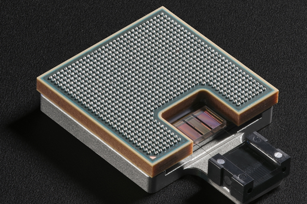
Fraunhofer IPMS has leveraged its experience from OLED-on-silicon technology for microdisplays to bring CMOS-integrated light sources of the highest pixel density and brightness, as well as the lowest power consumption, to a pixelated OLED microsensor that can individually control spatially distributed light channels assignable to corresponding audio frequencies in the cochlea via a serial interface.
Where was the challenge in developing the technology?
Although Fraunhofer IPMS has already introduced unique features with its OLED-on-silicon technology for microdisplays that are also important for optogenetics, there are still some challenges: The necessary brightness and degree of integration have been successfully demonstrated during the project. However, flexibility and biocompatibility are not yet verified. The silicon microtechnology used has shown that these properties are generally achievable. With further research and development effort, they also appear feasible here.
When will the technology be market-ready?
The project laid the first foundations for the use of OLED-on-silicon technology in optogenetics. The results are promising. The scientists will continue to work on this technology and remain open to other areas of application.


