Industry plans to invest $400 billion in 300mm fab equipment
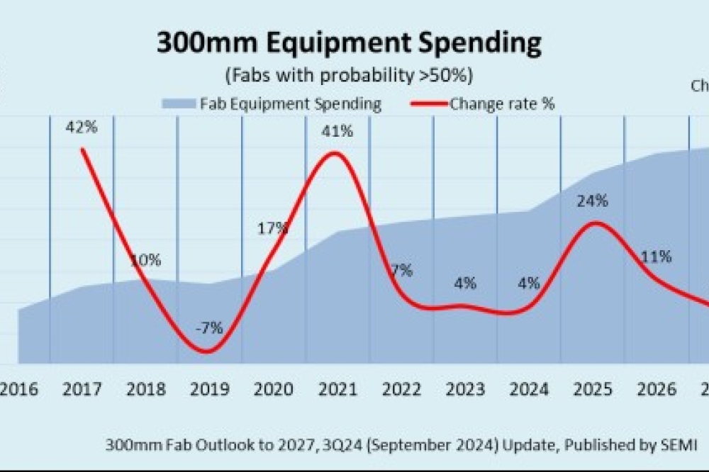
Global spending on 300 mm fab equipment is expected to reach a record US$400 billion from 2025 to 2027, SEMI has highlighted in its quarterly 300 mm Fab Outlook Report to 2027 report.
The robust spending is being driven by the regionalization of semiconductor fabs and the increasing demand for artificial intelligence (AI) chips used in data centers and edge devices.
Worldwide, 300mm fab equipment spending is projected to grow by 4% to US$99.3 billion in 2024, and further increase by 24% to US$123.2 billion in 2025, surpassing the US$100 billion level for the first time. Spending is forecast to experience 11% growth to US$136.2 billion in 2026 followed by a 3% increase to US$140.8 billion in 2027.
“The magnitude of the expected ramp of global 300mm fab equipment spending in 2025 sets the stage for a record-setting three-year period of semiconductor manufacturing investments,” said Ajit Manocha, SEMI President and CEO. “The world’s ubiquitous need for chips is boosting spending on equipment for both leading-edge technologies addressing AI applications and mature technologies driven by automotive and IoT applications.”
Regional Growth
China is projected to maintain its position as the top spending region on 300mm equipment globally until 2027, investing over US$100 billion in the next three years driven by its national self-sufficiency policies. However, spending is anticipated to gradually decrease from a peak of US$45 billion in 2024 to US$31 billion by 2027.
Korea is projected to rank second and invest US$81 billion in the next three years to further its dominance in memory segments including DRAM, high-bandwidth memory (HBM), and 3D NAND Flash. Taiwan is forecast to spend US$75 billion on 300mm equipment over the next three years, ranking third as the region’s chipmakers build some new fabs overseas. Leading-edge logic below 3nm is the primary driver of Taiwan fab investments.
The Americas is projected to invest US$63 billion from 2025 to 2027, while Japan, Europe & Mideast, and SE Asia are expected to spend US$32 billion, US$27 billion, and US$13 billion, respectively, over the three-year period. Notably, these regions are anticipated to more than double their equipment investment in 2027 compared to 2024 due to policy incentives earmarked to alleviate concerns on the supply of crucial semiconductors.
Segment Growth
Foundry equipment spending is projected to reach approximately US$230 billion between 2025 and 2027, fueled by investments in sub-3nm cutting-edge nodes as well as continued spending on mature nodes. Investment in 2nm logic processes and development of key technologies at 2nm, such as gate-all-around (GAA) transistor structure and back-side power delivery technology, is crucial to meet future high-performance and energy-efficient computing needs, particularly for AI applications. Cost-effective 22nm and 28nm processes are expected to see growth due to increasing demand for automotive electronics and IoT applications.
The Logic and Micro segment is projected to spearhead the equipment spending expansion over the next three years, with an anticipated total investment of US$173 billion. Memory comes in second, expected to contribute over US$120 billion in spending during the same period, marking the beginning of another segment growth cycle. Within Memory, investment in DRAM-related equipment is projected to surpass US$75 billion, while investment in 3D NAND is expected to reach US$45 billion.
The Power-related segment ranks third, with an expected investment of over US$30 billion over the next three years, including around US$14 billion for compound semiconductor projects. The Analog and Mixed-signal segment is projected to reach US$23 billion during the same period followed by Opto/Sensors at US$12.8 billion.


