Significant EU funding for VTT's semiconductor development
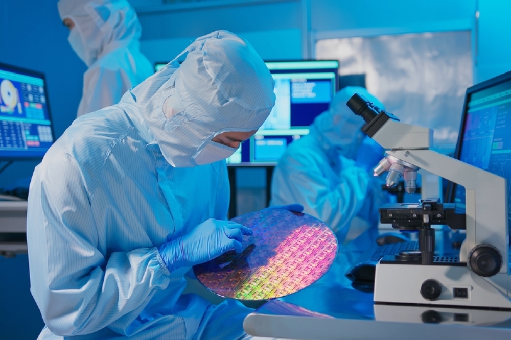
The Public Authorities Board of the Chips Joint Undertaking (EU Chips Act) has decided to fund European semiconductor pilot line proposals.
VTT is involved in two of the pilots that are about to start their operations. Its share of the funding will be used to purchase equipment for the shared-use Kvanttinova cleanroom to be built at Espoo, Finland. The pilot lines will support European chip technology development and chip production growth targets, and Finland will be strongly integrated into the European semiconductor industry ecosystem. VTT's shared-use cleanroom will allow companies to develop and pilot microelectronics components.
VTT Technical Research Centre of Finland is participating in two of the European pilot line projects that are aiming to strengthen development of the European semiconductor industry. Large European-funded pilot lines, FAMES and NanoIC, are operated by CEA-Leti in France and imec in Belgium. The lines will develop new semiconductor processes and technologies that will be accessible to companies for product development and scaling up to production. The technologies under development include the latest transistor and RF technologies and new memory technologies.
The 32 million euros in funding provided by the EU and the Finnish Government will be invested in VTT's shared-use cleanroom equipment and the development of semiconductor manufacturing processes.
“The recent EU Chips Act funding, together with funding provided by the Finnish Government last autumn, will ensure Finland’s involvement in pilot lines that are important to the European semiconductor industry. The development will support and strengthen Europe's role in the global chip market, and bring Finland into this ecosystem,” says Tauno Vähä-Heikkilä, Vice President, Microelectronics and Quantum Technologies at VTT.
Construction of the European pilot lines has already started and will accelerate with confirmation of the funding. The European pilot line equipment, operations and services provided by VTT will be integrated within Kvanttinova, a semiconductor and quantum technology RDI hub located in Espoo, Finland. Kvanttinova is a new RDI hub for microelectronics and quantum industry players in Espoo, currently at the peak of its planning stage. In addition, some equipment will be placed in the Micronova Centre of Micro- and Nanotechnology already located in Espoo. Services will gradually be offered to companies, and the first semiconductor processes in Finland are scheduled to start up in late 2026.
The recent Chips Act funding decisions and the resulting equipment acquisitions by VTT will support the strongest Finnish semiconductor industry competence areas, especially new materials, ALD (atomic layer deposition) technology for memory applications, and RF technologies.
“The Kvanttinova shared-use cleanroom will provide Finnish companies with the opportunity to develop materials, technologies, and innovations for new products and markets – without the need for significant investments. It will also give companies access to the services and processes of major European operators, such as CEA-Leti and imec,” says Pekka Pursula, Research Manager at VTT.


