Loading...
News Article

ZEISS Microscopy opens Semiconductor Applications Laboratory in Dresden

News

State-of-the-art innovation lab pushes the limits of advanced semiconductor applications.

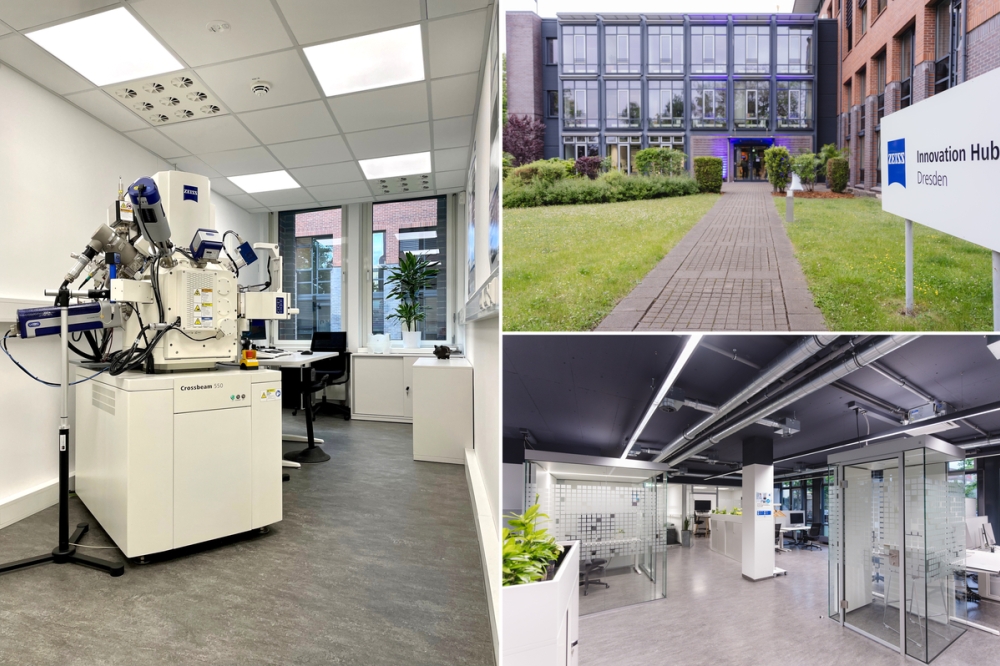
ZEISS recently opened the ZEISS Microscopy semiconductor applications lab in Dresden, a state-of-the-art facility dedicated to addressing physical analysis challenges and pushing the limits of nanoscale analysis with the ZEISS Crossbeam focused ion beam-scanning electron microscope (FIB-SEM).


The new facility is strategically located in Dresden, the heart of semiconductor innovation within Europe, allowing for close collaboration with semiconductor industry customers and partners on physical failure analysis, materials development and process yield improvement for advanced logic and memory, power semiconductors, MEMS, advanced packaging, and more. ZEISS will address increased automation of microscopy workflows and advanced techniques to help the semiconductor industry accelerate root cause analysis and pathfinding for the most challenging issues in microelectronics.

This laboratory in Dresden is the third major investment of ZEISS into semiconductor microscopy applications and strengthens the company’s global support capabilities. The Dresden team collaborates closely with its counterparts in Taiwan and Korea to share knowledge and best practices to best address customer needs across these three global hotspots of semiconductor excellence. Importantly, the advanced applications developed by these three teams will steer the innovation roadmap of ZEISS to meet the greatest challenges facing lab professionals in the semiconductor industry.

The semiconductor microscopy applications lab is located within the ZEISS Innovation Hub Dresden that opened last May. The site complements ZEISS’ Innovation Center in Hsinchu Science Park, Taiwan, which opened in June 2024 and features a comprehensive portfolio to meet the productivity needs of semiconductor research & development, production and failure analysis. The third Innovation Center is in Dongtan, Korea, where the company develops applications across a complete portfolio of optical and electronic equipment, X-ray microscopy and high-resolution CT, and 3D metrology instruments.

Silicon photonics: accelerating growth in the race for high-speed optical interconnects
CCD-in-CMOS technology enables ultra-fast burst mode imaging
2025 6G A look forward
Critical Manufacturing climbs Deloitte’s Technology Fast 50
Semiconductors: The most important thing you probably know the least about
Imec and partners unveil SWIR sensor with lead-free quantum dot photodiodes
Lattice introduces small and mid-range FPGA offerings
SEMI and SMT inspection solutions at NEPCON Japan 2025
Nordic Semiconductor and Kigen demonstrate Remote SIM Provisioning for Massive IoT
Spirent collaborates with Siemens
Quobly forges strategic collaboration with STMicroelectronics
New standards in pressure measurement systems for the semiconductor industry
IBM delivers optics breakthrough
Semiconductor equipment sales to reach $139 Billion in 2026
Marvell introduces 1.6 Tbps LPO Chipset
ACM research strengthens Atomic Layer Deposition portfolio
CEA-Leti demonstrates embedded FeRAM platform compatible with 22nm FD-SOI node
Lattice introduces small and mid-range FPGA offerings
Solace unlocks full potential of event-driven integration
Advantest to showcase latest test solutions at SEMICON Japan 2024
CEA-Leti device integrates light sensing and modulation
Nordic launches Thingy:91 X prototyping platform for cellular IoT and Wi-Fi locationing
Imec achieves seamless InP Chiplet integration on 300mm RF Silicon Interposer
High-precision SMU
Powering India’s energy future
China’s Nvidia probe puts global investors ‘on notice’
POET Technologies appoints new director
Imec demonstrates core building blocks of a scalable, CMOS-fab compatible superconducting digital technology
Imec proposes double-row CFET for the A7 technology node
ULVAC launches new deposition system
Beebolt and SEMI Announce Strategic Partnership to Drive Supplier Resilience and Agility
esmo group introduces Automated Final Test Manipulator
×
Search the news archive

To close this popup you can press escape or click the close icon.
Logo
x
Logo
×
Register - Step 1

You may choose to subscribe to the Silicon Semiconductor Magazine, the Silicon Semiconductor Newsletter, or both. You may also request additional information if required, before submitting your application.


Please subscribe me to:


You chose the industry type of "Other"

Please enter the industry that you work in:
 
X
Adblocker Detected
Please consider unblocking adverts on this website