
Accelerating semiconductor designs for AI applications
Expanded network-on-chip tiling supported by mesh topology capabilities in FlexNoC and Ncore interconnect IP products allow systems-on-chip with AI to easily scale by more than 10 times without changing the basic design, meeting AI's huge demand for faster and more powerful computing.
Arteris has announced an innovative evolution of its network-on-chip (NoC) IP products with tiling capabilities and extended mesh topology support for faster development of Artificial Intelligence (AI) and Machine Learning (ML) compute in system-on-chip (SoC) designs. The new functionality enables design teams to scale compute performance by more than 10 times while meeting project schedules plus power, performance and area (PPA) goals.
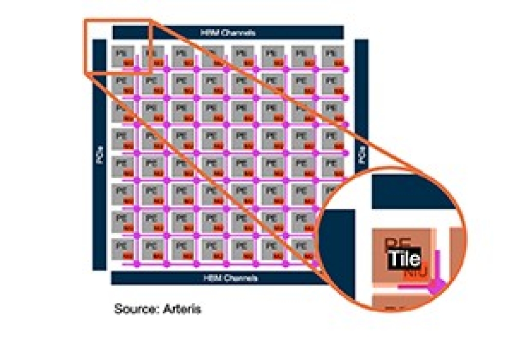
Network-on-chip tiling is an emerging trend in SoC design. The evolutionary approach uses proven, robust network-on-chip IP to facilitate scaling, condense design time, speed testing and reduce design risk. It allows SoC architects to create modular, scalable designs by replicating soft tiles across the chip. Each soft tile represents a self-contained functional unit, enabling faster integration, verification and optimization.
Tiling coupled with mesh topologies within Arteris’ flagship NoC IP products, FlexNoC and Ncore, are transformative for the ever-growing inclusion of AI compute into most SoCs. AI-enabled systems are growing in size and complexity yet can be quickly scaled with the addition of soft tiles without disrupting the entire SoC design. Together, the combination of tiling and mesh topologies provides a way to further reduce the sub-system design time and overall SoC connectivity execution time by up to 50% versus manually integrated, non-tiled designs.
The first iteration of NoC tiling organizes Network Interface Units (NIUs) into modular, repeatable blocks, improving scalability, efficiency and reliability in SoC designs. These SoC designs result in increasingly larger and more advanced AI compute which supports fast-growing, sophisticated AI workloads for Vision, Machine Learning (ML) models, Deep Learning (DL), Natural Language Processing (NLP) including Large Language Models (LLMs), and Generative AI (GAI), both for training and inference, including at the edge.
“Arteris is continuously innovating, and this revolutionary NoC soft tiling functionality supported by large mesh topologies is an advancement in SoC design technology,” said K. Charles Janac, president and CEO of Arteris. “Our customers, who are already building leading-edge AI-powered SoCs, are further empowered to accelerate the development of much larger and more complex AI systems with greater efficiency, all while staying within their project timeline and PPA targets.”


