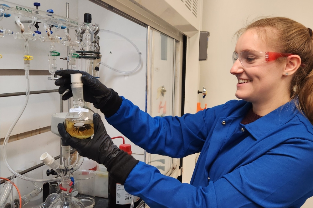
Terecircuits Corporation, a venture-backed startup in advanced materials for the semiconductor industry, has introduced Terefilm®, a patented material designed for temporary bonding and debonding applications in advanced packaging.
According to Boston Consulting Group: “The next generation of industry-leading organizations will be those that realize value creation is migrating towards companies that can design and integrate complex, system-level chip solutions using concepts like advanced packaging.” As components become smaller and more complex, the need for advanced temporary bonding materials, like Terefilm®, becomes paramount to enable emerging applications, including thin wafer handling and the transfer of fragile components.
Terefilm® meets these requirements, offering unparalleled advantages including rapid release, precise patterning, and clean decomposition without solvents. The material can be used in processing up to 230ºC, giving customers a wide process window for bond-debond with clean
decomposition.
“Our focus with Terefilm® is squarely on innovating a novel material that will enable faster and more accurate semiconductor advanced packaging and related manufacturing processes,” said Wayne Rickard, CEO of Terecircuits. “Its benefits for bonding and debonding in semiconductor advanced packaging are compelling, offering ultra-clean, ultra-fast and residue-free release that eliminates traditional cleaning requirements and accelerates production. At the same time, its ability to enable selective material removal at nanoscale positions it for use in such diverse applications as enabling the parallel transfer of micro-LEDs and a photoresist for direct-write lithography. This flexibility makes Terefilm® a valuable solution for the challenges faced in advanced packaging today as well as emerging ones across a wide range of electronics manufacturing requirements.”
The properties of Terefilm® make it highly effective for several critical applications:
• Clean Decomposition: Unlike conventional materials, Terefilm® undergoes a remarkably clean decomposition process when activated, leaving no residue. This ensures ultra-clean surfaces, which are essential for successful hybrid bonding and other high-precision applications.
• Rapid Release: Traditional heat and UV-sensitive films can take several minutes to release. Terefilm®, however, releases in microseconds. This near-instantaneous decomposition significantly enhances manufacturing efficiency.
• Precise Patterning: Similar to lithographic photoresists, the material can be patterned to enable selection of specific regions. This allows for the targeted release of individual chips or subsets of chips, replacing the traditional pick-and-place process. This capability enables the parallel transfer of multiple components, dramatically increasing production speed and precision.