Visualisation first for UC Santa Barbara

Researchers create the first ever visualisation of photoexcited charges traveling across the interface of two semiconductor materials.
UC Santa Barbara researchers have achieved the first-ever “movie” of electric charges traveling across the interface of two different semiconductor materials. Using scanning ultrafast electron (SUEM) techniques developed in the Bolin Liao lab, the research team has directly visualized the fleeting phenomenon for the first time.
“There are a lot of textbooks written about this process from semiconductor theory,” said Liao, an associate professor of mechanical engineering. “There are a lot of indirect measurements.” The ability to visualize how this process actually happens will allow semiconductor materials scientists to benchmark some of these theories and indirect measurements, he added.
The research is published in the Proceedings of the National Academy of Sciences.
‘Hot’ photocarriers
If you’ve ever used a solar cell, you’ve seen photocarriers in action: sunlight hits a semiconductor material, exciting electrons in the material, which move. This movement of electrons, and separation from their opposite-charged ‘holes,’ creates a current that can be harnessed to power electronic devices.
However, these photocarriers lose most of their energy within picoseconds (trillionths of a second) so that the energy that conventional photovoltaics harvests is but a fraction of the energy these carriers have in their “hot” state, before they cool down and release most of the excess energy as waste heat. While their hot state holds a lot of potential for things like energy efficiency, it also presents challenges within the semiconductor material, such as the heat that may affect device performance.
As a result, it’s important to get a good idea of how these hot carriers behave as they move through different semiconductor materials, and in particular how they move across the interface of two different materials — the heterojunction. In the realm of semiconductor materials, heterojunctions influence the movement of charge carriers for a variety of purposes, from the creation of lasers to photovoltaics to sensors to photocatalysis.
“The really exciting thing about this work is that we were able to visualize how the charges, once generated, actually transfer across the junction.”
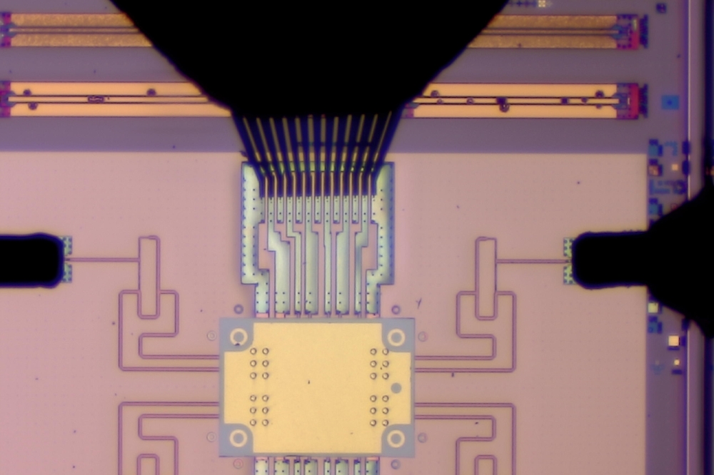
To visualize these hot carriers, Liao and his group focused their SUEM on a heterojunction of silicon and germanium fabricated by collaborators at UCLA, a combination of common semiconductor materials that holds promise in realms such as photovoltaics and telecommunications.
“Basically, we’re trying to add time resolution to electron microscopes,” Liao said.
Key to their imaging technique is their use of ultrafast laser pulses to act as a picosecond-scale shutter as they fire an electron beam to scan the surface of the materials through which the hot photocarriers travel, excited by an optical pump beam. “What we’re talking about are events happening within this picosecond to nanosecond time window,” Liao said.
“The really exciting thing about this work is that we were able to visualize how the charges, once generated, actually transfer across the junction,” he continued. The resulting images show these photocarriers as they diffuse from one semiconductor material to the other.
The movie shows a time series of SUEM contrast images taken after the Si/Ge heterojunction is excited by one optical pulse. The optical pulse generates negative and positive charges (electrons and holes) around the junction area, which then diffuse and interact with the junction electrical potential. White and black contrast in the images represent electron and hole populations as they evolve in space and time.
“If you excite charges in the uniform silicon or germanium regions, the hot carriers move very, very fast; they have a very high speed initially because of their high temperature,” Liao explained. “But if you excite a charge near the junction, a fraction of the carriers are actually trapped by the junction potential, which slows them down.” Trapped hot charges result in reduced carrier mobility, which can negatively affect the performance of devices that separate and collect these hot charges.
This charge trapping in Si/Ge heterojunctions can be understood by semiconductor theory but it was still striking to directly observe it experimentally, noted Liao. “We didn’t expect to be able to image this effect directly,” he said, adding that this phenomenon might be something semiconductor device designers may want to address. “This paper is really about demonstrating the capability of SUEM to, for example, study realistic devices.”
This new ability to actually see hot photocarrier activity at heterojunctions completes a circle in semiconductor research at UC Santa Barbara. Pioneered by late UCSB engineering professor Herb Kroemer, who first proposed the role of heterostructures in semiconductors, the concept went on to become the basis of modern microchips, computers and information technology. Kroemer received the 2000 Nobel Prize in Physics “for developing semiconductor heterostructures used in high-speed and opto-electronics.”

