
Heidelberg Instruments launches nanolithography tool
Heidelberg Instruments has launched its new NanoFrazor nanolithography system, advancing decades of expertise in micro- and nanofabrication.
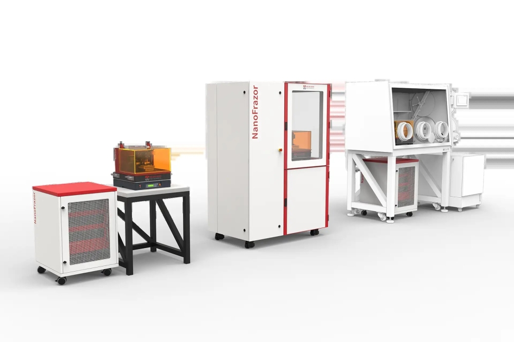
This versatile tool, designed for high resolution, flexibility, throughput, and modularity, can be equipped with ten parallel patterning cantilevers, significantly boosting productivity. Combining Thermal Scanning Probe Lithography (t-SPL), Direct Laser Sublimation (DLS), and enhanced automation, the NanoFrazor supports cutting-edge research in quantum devices, 1D/2D materials, and nanoscale electronics, as well as applications in nanophotonics, meta-optics, and nanofluidics.
At the heart of the NanoFrazor is an ultrasharp, heatable probe tip, enabling precise patterning of nanostructures with lateral resolutions as fine as 15 nm and vertical resolutions down to 2 nm. Its in-situ inspection system offers Closed-Loop Lithography (CLL), allowing for markerless overlay and real-time adjustments to ensure sub-2 nm vertical precision for even the most complex grayscale patterns. This groundbreaking feature enables advanced applications in photonics, biomimetic substrates, and local material modification through heat-induced chemical reactions or phase changes.
Key Features:
Thermal Scanning Probe Lithography (t-SPL): High-precision patterning for critical nanodevice components.
Modularity: The NanoFrazor’s configurable platform allows for tailored solutions based on application and lab requirements. Additional modules and upgrades can be installed as research progresses, offering flexibility and scalability.
Resolution & Throughput: With the new Decapede module, throughput is increased tenfold by utilizing 10 independent thermal cantilevers, delivering speed without sacrificing resolution.
Hybrid Mix & Match Lithography: The NanoFrazor supports a Direct Laser Sublimation (DLS) module for faster micrometer-resolution writing, making it ideal for large-area patterns like contact wires and pads.
Building on decades of R&D originating at IBM Research Zürich, the NanoFrazor continues to evolve at Heidelberg Instruments Nano. A comprehensive library of best practices in etching, lift-off, and other processes ensures that users can optimize their results across various applications.


