
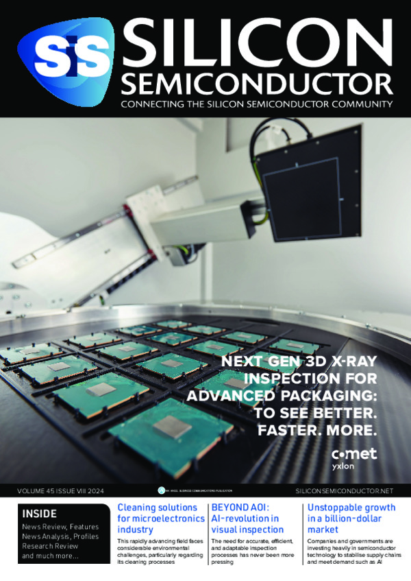
Next Gen 3D X-Ray Inspection for Advanced Packaging: To see better. Faster. More.
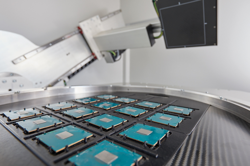
As 3D IC packaging becomes ever more intricate and demanding,
traditional inspection techniques are struggling to keep up. 3D X-ray
inspection, powered by AI, is transforming how manufacturers view their
products, offering a higher resolution without sacrificing speed or
damaging valuable samples.
By Joscha Malin, Director Product Marketing Software Solutions, Comet Yxlon
As the demand for miniaturization grows, semiconductor packaging design is rapidly evolving. Manufacturers are now incorporating 2.5D and 3D ICs into their production, pushing the boundaries of functionality within increasingly compact volumes. This shift brings new challenges, not only in designing robust initial prototypes but also in managing the higher manufacturing and material costs associated with more complex structures. To maintain a competitive edge, manufacturers must adopt comprehensive inspection strategies that help increase yield and accelerate time-to-market without compromising on reliability.
Crucial to the success of these inspection strategies is the ability to detect defects early within the design and manufacturing process. The sooner manufacturers can identify and resolve issues, the faster they can scale up production, ultimately leading to improved yield and a faster path to market success. This is where advanced inspection technologies, particularly 3D X-ray inspection, come into play.
Bridging the Gap with 3D X-Ray Inspection
Historically, inspection methods for 3D ICs have relied on three primary technologies: optical inspection, 2D X-ray, and focused ion beam scanning electron microscopy (FIB-SEM). Each technology brings its own strengths and weaknesses. Optical inspection offers speed and repeatability but lacks the level of detail necessary for comprehensive 3D analysis. FIB-SEM provides unmatched resolution, but it’s a slow, destructive process. Meanwhile, 2D X-ray falls in between—offering non-destructive insight but often lacking the speed or resolution required for today’s complex 3D IC structures. 3D X-ray inspection fills the gap between these technologies, delivering detailed, non-destructive insights in a fraction of the time required for a FIB-SEM analysis. What’s driving its rise now, especially for advanced semiconductor packaging, isn’t just the improvement in X-ray hardware, but the breakthroughs in software and AI that support it.
As 3D IC packaging becomes ever more intricate and demanding, traditional inspection techniques are struggling to keep up. 3D X-ray inspection, powered by AI, is transforming how manufacturers view their products, offering a higher resolution without sacrificing speed or damaging valuable samples. By harnessing AI-driven image analysis, 3D X-ray technology can detect even the smallest defects, like voids or misalignments, with incredible precision. These systems use advanced reconstruction algorithms and data segmentation techniques to reveal fine details inside complex structures. AI further accelerates this process, providing insights at a scale and speed that were previously unattainable, ultimately boosting yield and quality.
The Three Pillars of Effective Inspection: Clarity, Efficiency, and Insight
For any inspection technology to be successful, it must excel in three key areas, all heavily dependent on software:
Clarity: This refers to the quality of the captured image, particularly how well the technology can visualize small details within complex structures. In the case of 3D X-ray, the combination of high-quality hardware and advanced reconstruction algorithms ensures exceptional image clarity, making even minute defects visible.
Efficiency: Automation plays a vital role here. The ability to quickly gather and process images into usable data can significantly reduce inspection times and improve throughput. AI enhances this by automating much of the defect recognition process, allowing operators to focus on critical decision-making rather than manual inspection.
Insight: Beyond what is visible to the eye, the real value lies in the data derived from the images. Advanced software can interpret this data to provide actionable insights, allowing manufacturers to make informed decisions. For instance, defects such as voids in solder bumps or “head-in-pillow” issues can be precisely measured and categorized, offering clear guidance on whether they fall within acceptable parameters.
The beloW scan of a commercially available CPU (figure. 1), captured with Comet Yxlon’s CA20 inspection solution, highlights what is already possible with today’s technology, revealing detailed information about C4 bumps, including defects such as voids of only 10 microns in diameter. These scans take just minutes, highlighting the speed and precision of modern 3D X-ray technology

Figure 1: A close up rendering of C4 bumps (diameter: 65µm) within a
commercially available CPU. All image property rights remain with Comet
Yxlon and images are not to be copied or distributed.
In another example, a “virtual slice” is taken from a reconstructed 3D volume of a GPU, allowing users to view 2D cross-sections of different layers within the chip, including C4 bumps, interposer bumps, and high-bandwidth memory (HBM) bumps (figure 2). This type of detail would be highly challenging to obtain with optical inspection or 2D X-ray due to the stacked nature of the layers obscuring underlying features.
While capturing high-resolution images is critical, the true power of 3D X-ray lies in the AI-powered software behind it. Assisted defect-recognition software such as Comet Yxlon’s CoS Insights package can rapidly detect and analyze the size and severity of defects, such as solder bump misalignments, and head-in-pillow issues. By measuring key parameters, like bump shift, die tilt, and the likelihood of defects forming, this technology provides a comprehensive understanding of the part’s condition, allowing manufacturers to spot these defects early and prevent costly issues down the line.

Figure 2: Left, virtual slice of a reconstructed X-ray scan of a
commercially available GPU with 100µm C4 bumps, 30µm microbumps and 20µm
high bandwidth memory bumps. Right, virtual slice of a reconstructed
X-ray scan of a commercially available CPU with ca 65µm C4 bumps. All
image property rights remain with Comet Yxlon and images are not to be
copied or distributed.
Insights: Taking stock of what’s within
Even early in the ramp-up process, where initial designs are being manually tested in small batches to a late stage before entering mass production, assisted defect recognition can be a valuable asset, providing repeatable, transferable results based on captured data.
As with any software to be used within an industrial context, the focus lies in delivering critical information as efficiently and as clearly as possible, to ensure a variety of experts across different levels can maximize the value of the solution and understand the results. Comet Yxlon have worked closely with Dragonfly, Comet’s AI brand with roots in Montreal, Canada, to develop a range of software-assisted workflows within the semiconductor space that utilize deep learning to streamline inspection workflows. Training the bump inspection within the software takes just four simple steps:
Step 1: The user chooses the desired solder plane for analysis. The software can suggest which solder planes might be of interest based on previous data and adapts to previously set preferences.
Step 2: The software is trained to recognize the bumps within the chosen sample. After manually defining the first few examples, the software will then analyze the entire sample and find all relevant bumps within the defined parameters.
Step 3: As with step 2, the software first needs to be told the parameters it is working with to find the connection to a substrate or interposer die. Once defined, it will identify these connections automatically.
Step 4: Once the parameters have been defined, the results are provided as a report, and in a machine-readable format.
This set-up, of just a few minutes, only needs to be defined once for a particular batch/part type. The outcome of this process is shown in figure 3. In this image, taken from the software, the segmentation of a particular plane is shown, with green and red indicators used to visualize the performance of each bump within pre-defined limits. This particular example is the result of the shift and tilt and head-in-pillow evaluation, where it is clearly visible that all bumps have shifted slightly, with the bump shown in red exceeding the given limits for maximum shift.
To determine this shift, the software precisely evaluates every recognizable bump across several key metrics, analyzing the direction and the length of the shift. To determine die tilt, the stand-off height is measured, and for the head-in-pillow, an indicator is provided for the likelihood within each bump. These values, if used correctly, can be vital for identifying trends even before actual head-in-pillow defects appear.

Figure 3: Bumps automatically inspected by CoS Insights including a bump
highlighted due to the violation of maximum shift allowed. All image
property rights remain with Comet Yxlon and images are not to be copied
or distributed.
Optimizing New Product Introductions (NPI) with 3D X-Ray
Alongside providing value in the lab, a thorough inspection strategy that includes 3D X-ray can lead to significant yield improvements during the new product introduction phase. By detecting and addressing defects early in the ramp-up process, manufacturers can rapidly optimize their production line and achieve higher yields. In the hypothetical scenario shown below (Figure 4.), incorporating 3D X-ray into the inspection process resulted in a noticeable improvement in yield within just six months.
A dip in the yield curve can be seen around month 5, representing a major production issue. 3D X-ray technology can be beneficial in helping to speed up learnings from this expected setback, providing real-time monitoring across the production samples and sharing key information regarding their performance, helping identify the early signs of a developing trend before it becomes a problem.

Figure 4: A real-life yield curve and hypothesized gains using 3D X-ray inspection. All image property rights remain with Comet Yxlon and images are not to be copied or distributed.
Key Takeaways
3D X-ray inspection, especially when combined with AI-driven software, is revolutionizing semiconductor manufacturing. From early design and prototyping to mass production, this technology provides critical insights into defects that were previously difficult or impossible to detect. By integrating 3D X-ray into their inspection strategies, manufacturers can improve yield, reduce time-to-market, and ensure higher reliability in their products. This powerful combination of hardware and software, in this case Comet Yxlon and Dragonfly, is not just a tool for today but a key enabler for the future of semiconductor production.
Eager to discover more? Then join us in Munich at the SEMICON EUROPA 2024, in hall C2, Booth: 555.


