Splitting hairs to ten to the power of four
14ACMOS: EU project for the next technology node in semiconductor manufacturing.
By Mathias Winter, Head of Piezo Drives & Systems Technology, Global Research and Markus Wiederspahn, Corporate Communications, PHYSIK INSTRUMENTE L.P. (PI).
The 14ACMOS project is part of Horizon Europe, the EU’s key funding program for research and innovation for the period of 2021 to 2027 with a volume of more than € 95 billion. It tackles climate change, helps to achieve the UN’s Sustainable Development Goals, and boosts the EU’s competitiveness and growth.
Horizon is divided into six clusters, of which cluster 4 addresses “Digital, Industry & Space”, funded with more than € 15 billion. With a total of currently 127 projects cluster 4 aims to strengthen the competitiveness of European companies in semiconductor and photonics industries.
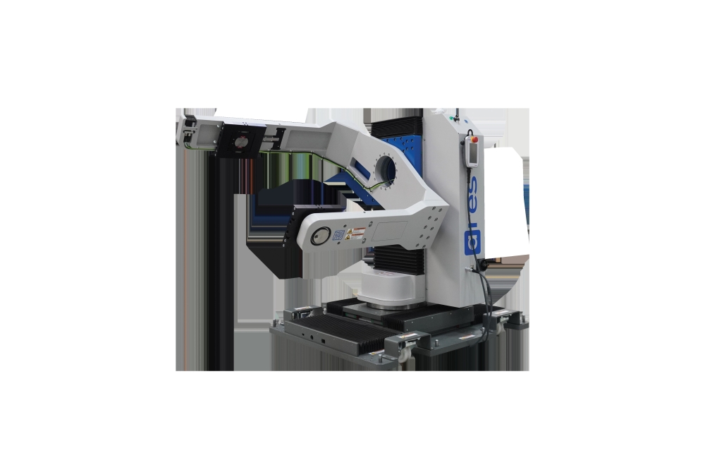
Application examples of magnetic direct drive technology.
The 14ACMOS project (14ACMOS = 14 Angstroem Complementary Metal-Oxide-Semiconductor) within Horizon aims to develop solutions for the 1.4 nm process technology node. Project activities address four key pillars: lithography, metrology, mask-infrastructure, and process technology.
Lithography solutions will be pushed to meet 1.4 nm capability, and extreme UV plasma physics will be studied to optimize optics transmission and lifetime. In the metrology pillar, advanced methods will be developed to improve measurement sensitivity and uncertainty and to assess reticle degradation induced by extreme UV light. Mask-infrastructure will cover the development of mask repair strategies based on particle removal technology and will assess durability. Process technology involves the development of patterning solutions, active device selection, and new interconnect technology, which are suitable for the 1.4 nm technology node.
The 14ACMOS project started in December 2022 and is set to end in November 2025. Total cost of the project sums up to € 94.6 million with an EU contribution of € 21.8 million. The project is coordinated by ASML. Participants are among others Carl Zeiss SMT, Trumpf, Applied Materials, KLA, Physikalisch-Technische Bundesanstalt (PTB).
European players like ASML, Carl Zeiss SMT, and PI have contributed to every step of miniaturization in semiconductor manufacturing along the way from several microns down to the 1.4 nm node. To reach precision of 1.4 nm, new actuator and motor concepts, sensors and (control) algorithms for the drives must be developed, besides advancements
in process technology, improved optics, and materials.
This project is co-funded by the European Union under grant agreement No 101096772 and is supported by the Chips Joint Undertaking and its members.
“Funded by the European Union. Views and opinions expressed are however those of the authors only and do not necessarily reflect those of the Chips Joint Undertaking. Neither the European Union nor the granting authority can be held responsible for them.”
PI offers 50 years of experience in piezo technology and nano positioning, a broad technological spectrum, and a high level of vertical integration in order to develop and provide components and systems that are optimally tailored to the respective process: From the very beginning, the basis for this consisted of mechanical motion systems (actuators and motors) and the appropriate bearing technology, sensors for recording the distance traveled and for determining the absolute position, algorithms for the firmware and an extensive collection of software interfaces and control technology. As a decade-long system partner of semiconductor equipment manufacturers and in particular the main participants in the 14ACMOS project, PI contributes its expertise and experience to the development of innovative motion solutions. The focus here is on very demanding motion and positioning tasks that require precision in the nanometer and sub-nanometer range. A particularly important aspect of some of the applications is the need to operate the systems under vacuum conditions. PI also offers suitable technologies and options for this.
The new N-332 linear stage utilizes the PiezoWalk® technology.
A wide range of drive technologies
The field of semiconductor manufacturing, and the 14ACMOS project in particular, presents a unique challenge for motion systems: the combination of long travel distances (up to hundreds of millimeters) with high dynamics, speed, and precision down to the nanometer range. PI meets these challenges head-on with a comprehensive portfolio of drive technologies.
Electromagnetic drives
In the class of electric motors, PI offers rotating electric motors such as DC or stepper motors. These are used in connection with screw or worm drives. Stepper motor systems with high-resolution encoders can perform minimum incremental motions of 10 nm with high reliability and repeatability.
Also, in the field of magnetic direct drives, a wide range of technologies is at hand, namely voice coil motors, iron-core and ironless linear motors, and torque motors.
Piezo-based actuators and drives
The motion of piezo actuators is based on solid-state effects, giving them unlimited resolution in principle. Their stiffness is very high, enabling high force generation and dynamics. Their rapid response time in the microsecond range is a result of their high resonant frequency which can reach more than one hundred kilohertz. Actuator travel in the range of several ten micrometers can be mechanically amplified to reach more than 1 mm. The combination of extremely high resolution and small travel ranges requires the use of suitable guiding elements which are typically flexures that enable highest accuracy by avoiding friction, play and backlash.
The PIOne optical nanometrology encoder from PI offers resolution down to 20 picometer RMS and better.
Piezo actuators, that are preloaded against a guided runner can be utilized to build linear motors with motion resolution of far below one nanometer. PiezoWalk® piezo motors from PI offer unique capabilities which perfectly match with the needs of semiconductor manufacturing. This nonmagnetic, vacuum-compatible, and clean-room-compatible technology is based on more than 30 years of experience with the development and production of piezoceramic components. PI received the SEMI Technology Innovation Showcase Award for the PiezoWalk® technology in 2005. The drives are continuously developed further, and a large number of variants are now available for different areas of application.
Resolution of these drives goes down to 30 picometer, travel ranges are scalable due to scalable runner length. Feed forces are in the range of 50 N to several 100 N. These drives are self-locking when switched off thus saving energy and reducing the generation of heat.
The latest addition to this product family, the N-332 linear stage, is configurable for use in multi-axis setups involving the X, Y, Z axes, and the XY, XZ, and XYZ planes. For applications that require operation in vacuum, the N-332 stages are available in configurations suitable for pressures as low as 10-9 hPa. The PICMAWalk piezo motor inside the N-332 stage is based on PI’s proprietary PICMA® piezo actuators.
A highly specialized application of piezo-based components are so-called PIRest actuators. With a load capacity of up to 4000 N per actuator and micrometer displacement with nanometer resolution, these components are ideally suited for drift compensation in machines, for alignment of optical components and static precision positioning.
Sometimes it is even necessary to combine motion systems that enable long-stroke movements, such as linear drives or piezo motors, with piezo-based actuators. Actuator and drive technologies are only one aspect considering the overall system properties. Optimal performance as required in applications targeted in the 14ACMOS project can only be achieved by implementing new and sophisticated control algorithms and the next generation of high-resolution sensor technology.
Magnetic levitation is a promising technology for high-precision motion in six degrees of freedom.
The right position sensor technology
Position sensing systems are required to provide feedback to the motion controller. Linearity and repeatability of motion and positioning tasks are not possible without highest-resolution measuring devices. Accuracies in the range of a few nanometers and below require a position measurement method that can also detect motion in this range. PI can also draw on extensive experience and a comprehensive portfolio of technologies developed in-house in this discipline. Examples comprise capacitive sensors and optical nanometrology encoders. The latter achieve a resolution of 20 picometer and better due to their small signal period of 500 nm and the optimized signal processing.
New magnetic levitation stages
The PI Group is committed to meeting the demanding objectives of the 14ACMOS project through the enhancement of existing technologies and the creation of novel and transformative new solutions. PI is also engaged in the development of new technologies beyond the scope of the 14ACMOS project. One illustrative example is that of magnetic levitation (maglev) stages with six degrees of freedom. One major benefit of this technology is the avoidance of any friction in the process chamber, eliminating the risk of particle contamination.
To employ this principle for the execution of high-precision movements, the magnets in the base are designed as electrically controllable coils. In order to enable movements in all six degrees of freedom, a corresponding number of magnet pairs is required. In a multitude of practical applications, Halbach arrays are employed to reduce energy consumption, augment load capacity, and diminish heat dissipation.
The combination of magnetic guidance and dedicated high-precision drive and sensor technologies provides high dynamics and the highest resolutions down to the picometer range. Active control and definition of guiding characteristics in up to six degrees of freedom can enable additional correction tasks such as focusing in Z or adjusting tip/tilt during operation. The frictionless guiding principle, which is free of rolling elements, lubrication, and air flow, will ensure the highest precision over the entire service life and allows use in cleanroom environments.
Controller technology
As demands on the precision, dynamics, and speed of mechanical motion systems increase, so too does the complexity of the control systems. The selection of an appropriate control technology is therefore of paramount importance. In particular, the control of piezo actuators and piezo-based positioning systems requires a high degree of specialization. PI has gained extensive experience in this field over decades. The characteristic properties of piezo actuators include the generation of large forces and fast response. In electrical terms a piezo element corresponds to a capacitance. A rapid change to the operating voltage brings about a rapid displacement of the actuator and thus a change in position.
When the control voltage suddenly increases, the piezo actuator can achieve its nominal displacement in only a few microseconds. A prerequisite for this is that the power supply provides sufficient current to charge the capacitance. For steady state operation, i.e., when holding a certain position, the stability of the power supply is crucial, as the piezoelectric actuators already respond with motion to the slightest voltage changes. Noise or drifting must therefore be avoided as far as possible.
With all these special features, PI benefits from more than 30 years of experience in the manufacture of piezo elements and the development of piezo-based positioning systems. PI is one of the few companies in the world with access to the entire value chain: from piezo development and production to the development of piezo-based motion systems and control technology.
PI can also look back on an even longer history of innovation in electric motor control technology. In addition to own cutting-edge solutions, PI leverages the expertise of ACS Motion Control, a wholly owned member of the PI Group based in Israel.
Magnetic levitation stages exemplify the necessity for sophisticated control technology. In this context, the linear stage platform is not constrained by mechanical bearings, allowing for unimpeded movement within a single degree of freedom. Consequently, a robust multi-axis controller with a high bandwidth is essential to maintain control over all other degrees of freedom.
Conclusion
The 14ACMOS project presents completely new challenges and tasks for all involved. Precise positioning plays a key role in many processes. For example, in the manufacture, inspection (quality control) and repair of lithography masks. In wafer inspection, it supports the detection of structural failures, defects and particles. Precise positioning is also essential in the lithography process, and in wafer metrology, for example for measuring layer thicknesses and overlay offsets.
With a comprehensive portfolio of precision positioning technologies and complementary expertise in sensor, control, motion and force transfer technologies, PI is well positioned to support this technology node.
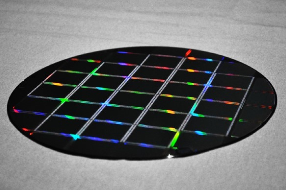
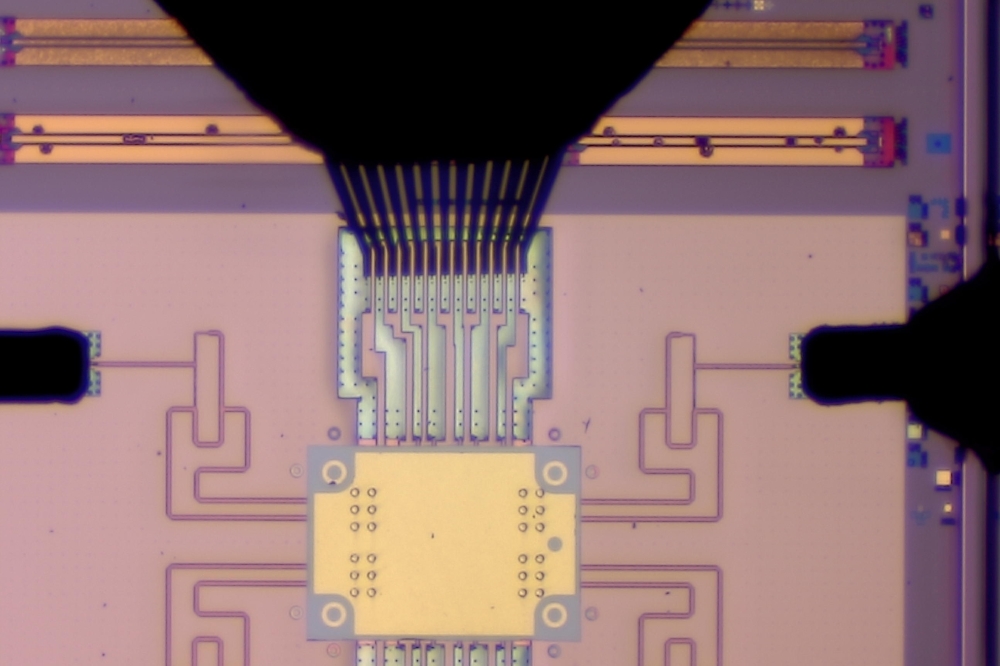
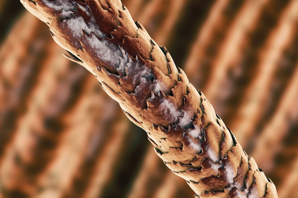
Main image: A human hair measures around 80 µm in diameter. The target size of the technology node in the EU-funded 14ACMOS project is more than ten thousand times smaller.


