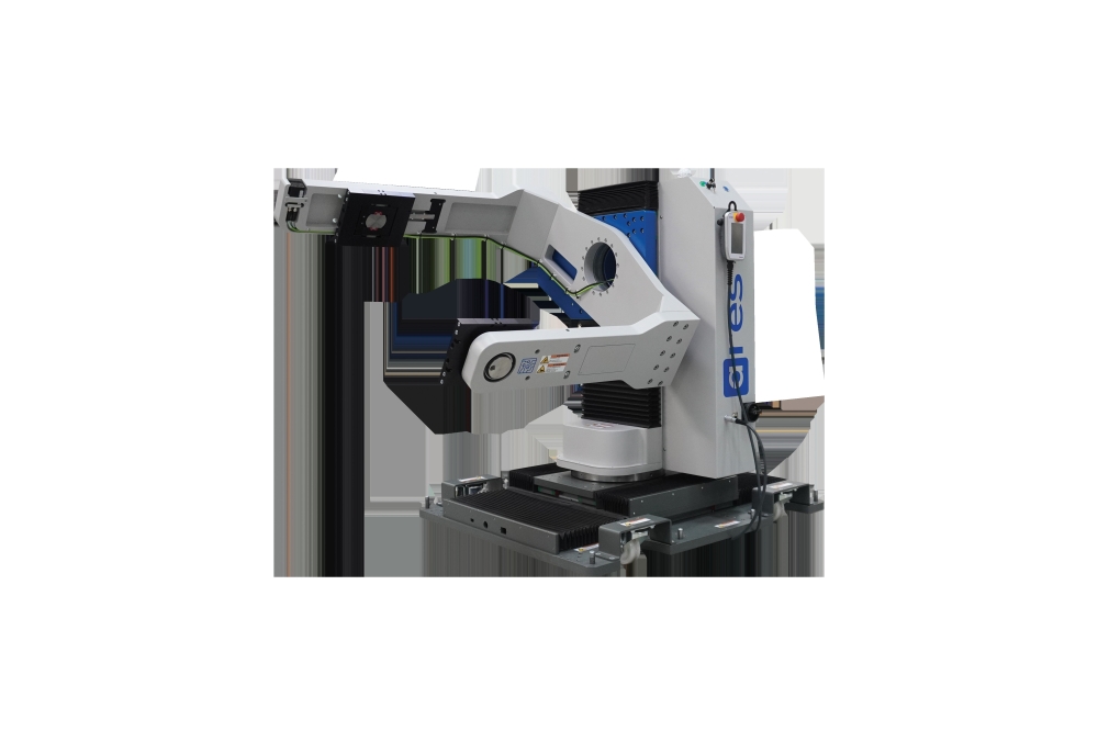
Test early and test often
EMANUELE BARDO, VICE PRESIDENT FOR THE SEMICONDUCTOR AND MEMS TEST BUSINESS UNIT AT SPEA, talks to Silicon Semiconductor Editor, Philip Alsop, about the importance of power semiconductor testing. He also explains the company’s expansion plans in Asia, and outlines SPEA’s ongoing track record for innovation, sharing some fascinating future roadmap plans.
PA: Power semiconductors are very much in the spotlight as the global focus on electrification is increasing, I won’t say exponentially, but very significantly?
EB: Yeah, this is exactly what SPEA is seeing. We are seeing an exponential global growth in the power segment, driven by three major factors - electrification, so EV and hybrid cars - as well as all of the business related to energy saving for consumers, as well as for solar panels. We see this trend growing all over the world, so in the United States, in Europe. But the biggest growth that we have seen is in Asia, and China in particular. I think this is well known. The investment made by Chinese companies in terms of power, with the support of the Chinese government, has been extremely significant in the past years. And this has been reflected in the amount of capital equipment that has been purchased and delivered.
PA: Alongside this electrification and the growing importance of power semiconductors, it follows that power semiconductor testing is becoming increasingly important in this world. In simple terms, we’re looking at performance and reliability when it comes to power modules or wider solutions?
EB: Correct. Being a brand new business, there was not the culture of high power testing consolidated in the same way it is today consolidated for memory or for mixed signal or for high performance digital. For us, this was a big challenge because first of all, we have to educate our customers in terms of the need for testing and how to test the products. The second big challenge, as you correctly mentioned, power modules - our products can go up to 10K volt, 20K volt, 10K amp. So, it is a completely different way of conceiving the test equipment because the reliability and the safety become two of the major items on which we need to focus as well as, of course, the performance, because all these products that are used - especially in the automotive market and especially the silicon carbide products - are extremely high voltage products with an extremely very fast switching time. The challenge is on all the elements - the reliability of the equipment, the safety of the equipment, as well as the technical performance. On top of this, educating the customer that testing is needed in all these areas.
PA: A single fault or a faulty component can ruin a power device or power solution - there are a range of damaging consequences?
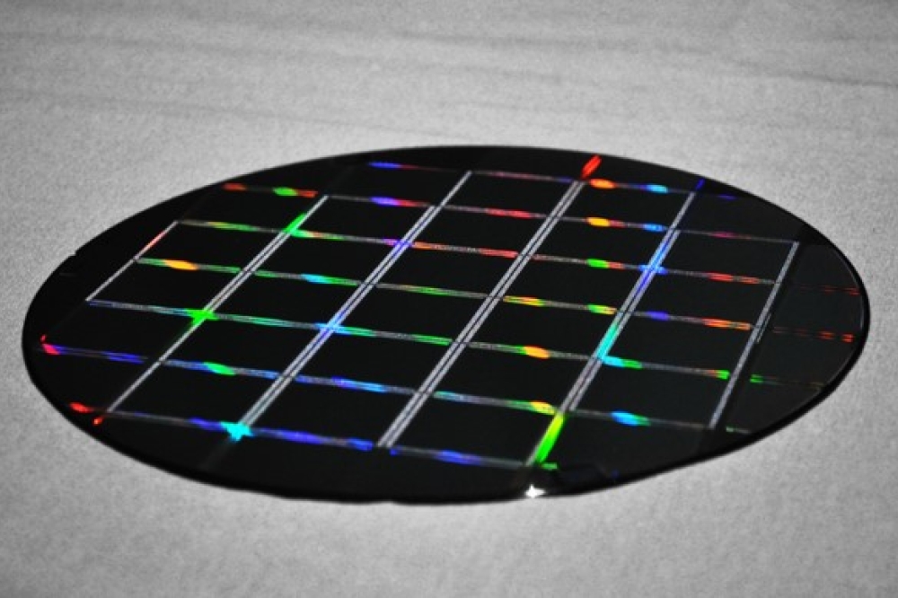
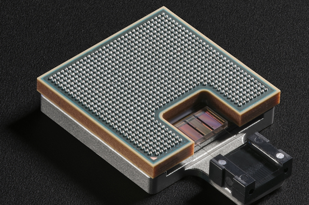
EB: Absolutely. A faulty component can cause an explosion. This is the reason why testing is needed from the very beginning. We don’t want the customer to assemble a full module and then discovering that the module is failing with consequences of, say, an explosion and with a cost that is significantly high. If you compare the average cost of a semiconductor chip and the cost of a power module, there is a factor of 100. It is absolutely vital to start testing in all the steps of the production. Testing on the wafers, testing at a single die level, the so-called KGD, testing on the DBC, so on the substrate, and finally testing the module and the package, in order to have the maximum yield in every step and in order to move the chips that have passed the test to the next step of the process.
PA: You’ve explained the need for continuous testing throughout the process. The traditional tests would include static parameter testing? Do you want to say anything about the benefits and any drawbacks of this?
EB: Historically, with this type of product, they were always doing the so-called static test. Also on the wafer, the majority of the tests are purely static. They simply verify that the component has not suffered major damage. When we say static test, it means applying high voltage in a static way and to measure a leakage current or to apply a high current and measure a voltage, as well as measuring the gate threshold voltage of the chip. These are tests that give you good information about the reliability of the process. However, static parametric test is not a functional test. We are not putting the device in real working conditions. If you think that these are IGBTs or MOSFETs, which are switches, the real working condition is to switch using the gate and to switch on and off. And when you switch on and off, you have a high voltage and high current that are flowing simultaneously in the device through the test equipment. And of course, at that point you have to measure all the parameters of the switching. The time that is necessary to switch from low current to high current and vice versa.
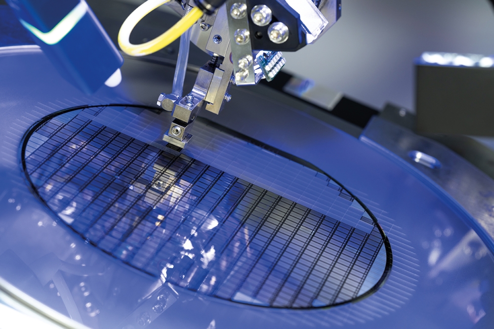
This brings the challenge which is the next step - the so-called dynamic test or switching test with the top performance that is the short circuit test. The problem, the technological problem, is that when you test on the wafer, some types of dynamic testing are not possible due to the environment, especially due to the parasitic element that is the chuck where the wafer is placed on. And this brings the need, the special need for this product to have an additional step of testing that is the bare die, the so-called KGD. Being able to extrapolate the single die from the wafer, at that point, it is possible to test static and dynamic directly on the die, to really check 100% the functionality of the product. Of course, this brings a big issue in real capability - you can imagine if one die is failing, you have a probe card with needle contacting and, if the equipment is not properly designed, you risk melting the needle as well as the wafer and all the conducting portion. That is the big challenge.
PA: You’ve explained the need for the dynamic performance evaluation. There’s a need for isolation testing as well. Can you say a little bit about where that comes into play?
EB: The isolation test is a test that is not performed at high level because it’s a test that measures the isolation through the external packing. But for sure, when you go in the final stage, so in the assembling the packaging, that can be a standard package like in the past or a more complex power module, the production line has to be equipped with isolation testing that has to be independent due to the fact that all the pins of the device have to be shorted together. This brings a challenge for our customers, because it’s a separate station with an additional cost, of course, and both static and dynamic testing, not necessarily only done at ambient, but, in certain situations, also done at temperature because we are talking of electrification and the majority of this business is related to automotive. And, as a whole, for the automotive requirement, the temperature testing is becoming much, much more important to guarantee the reliability over the time of the final product.
PA: To re-emphasise, you’ve outlined the steps of the testing, but the most important thing overall is to ensure that the testing is carried on throughout the process, as the solution is built up You’re testing at every stage and your message is ‘Test early and test often’?
EB: Correct. So, don’t just test the final product, because you cannot guarantee the performance as well as the reliability over the time of the full process, and it will absolutely not be cost-effective. Test early and test as much as you can in all the steps in order to have the better yield and in order to have a product that has a high reliability in the field and doesn’t risk premature failing.
PA: Presumably, the basic problem is if you only test at the end and you find a problem, it’s very difficult to then chain back to find out where the problem might lie, whereas if you’re testing frequently, you will hopefully come across a problem early on, and therefore you can deal with it so that you can then carry on building the solution, confident that it’s going to be working, as opposed to, suddenly at the end it doesn’t work, and then how do we find the problem?
EB: Exactly. Because, if you only do the final testing of the model and you discover that it has a yield of 60% or 70%, you don’t know which step(s) of the previous processes are causing this low yield. It’s very difficult to feedback on your internal process. Having the testing on wafer, on single die, on substrate, on so-called DBC, and finally in the module, you are able to feedback each step of your process and to understand which one has to be improved.
PA: In terms of the solutions available to do the testing that we’ve discussed, I guess SPEA is very well positioned for testing power semiconductors. I know you have the slogan or your concept is reimagining semiconductor testing. Can you just talk us through the solution or solutions that you think are particularly well suited to the situations we’ve discussed?
EB: If I look at the data, SPEA is number one in this specific field of high power testing. High power testing is knowledge that you cannot build in a very short time. We have departments that have studied the high power instrumentation of our equipment almost since the foundation of SPEA, because high power equipment has to be conceived and designed as high power since the first drawing and the first schematic of the equipment. It cannot be a mixed signal equipment where you add a certain power instrumentation. It will not work. The flexibility of the solutions we have in the field, gives our customers the possibility to have a single model of machine extremely scalable, so capable to be configured for each step of the testing, with even a single software and a single test programme that can run from wafer level until the package test. This is extremely important for our customers because they have the same machine that can perform all the steps of testing, and they can easily compare data, limits, and capability of testing. This has placed SPEA as a leader in the market for high power testing. For example, almost 40% of the EV market in China is tested on our machine.
PA: So far we’ve concentrated on power semiconductor testing. I know that’s a major focus for yourselves, but you are doing other things as well. Perhaps we can have a brief look at some of those - areas like automatic probe card testing, I think there’s some MEMS, environmental sensors testing, and we can’t ignore that the world is going ‘AI mad’ and there’s a need for testing for microchips for AI applications. Clearly, they’re big subjects in their own right. But can you at least give us a flavour of what you’re involved with in terms of each of these?
EB: There are two market segments where SPEA is leader. It is related to high power, as we correctly mentioned, and everything is sensor and MEMS. You mentioned environment. It is just one of the latest challenges that we are faced with. We have been awarded by many companies as a supplier to test, accelerometer, gyroscope, pressure sensor, high-g sensors, and so on.
These two represent almost 50% of the turnover for SPEA. Then, we are growing all over the world, the business related to analogue mixed signal, as well as high computing digital devices. If you think, all the AI chips are chips that must have a big capability to transfer data at high speed with a lot of power supply. And this is a market segment that for us is growing significantly. On top of this, we have recently approached the market with some, let’s say, very innovative equipment. For example, with a wafer prober it is no longer just a single probe card, as is already well known in the market.
There are certain devices, and this is one application, for some power chips like IGBTs or diodes, where there can be a certain technological advantage to probe both sides of the wafer, so top and bottom. We have also introduced equipment that has multi-probe cards, up to eight probe cards that can fly on the wafer and contact top and bottom. It’s a new technology that we strongly believe will grow in the future.
PA: Before we finish, I know SPEA Thailand is a new-ish venture, so it’d would be good to understand what’s going on there. And, if memory serves, I think it’s the 10th anniversary of your presence in China. I believe as part of the celebrations for this, you’ve actually expanded significantly the Suzhou facility. If you can talk us through a little bit about Thailand and then China?
EB: SPEA Thailand was opened at the beginning of May of this year. Thailand is one of the biggest installed bases for SPEA in Southeast Asia. SPEA has been present in Singapore for more than 20 years, and we also have service centres in Thailand, in Philippines, and in Malaysia. The decision of the company has been for a massive investment, first in Thailand and the Philippines will follow, to create offices, but especially to create the hub for all of our repair centres for Southeast Asia. So, the opening of SPEA Thailand is really important and strategic for the growth of all the businesses in Southeast Asia in order to better serve our tremendous installed base.
In terms of China, all the SPEA management was in Suzhou recently. SPEA has been present in China for 10 years and we celebrated this anniversary. Alongside this celebration, we also had a ceremony to open a new facility in Suzhou, a 2000 square metre facility with a demo room with more than 30 machines, a repair centre that will support all the mainland China business, and a plan to grow our personnel up to 200 people in China in terms of customer support, application and sales.
Today, China is the number one market in terms of revenue for SPEA. Historically, the relationship between Italy (we are an Italian company, of course!), and China has always been extremely good. And this positions SPEA extremely well for partnership with a major Chinese company. As you know, investment in China for independence on the semiconductor side is extremely high at the moment. We already have partnerships with a lot of companies, and we believe that this market will be an additional booming market for us in the next 10 years.
PA: What we’ve discussed, you’re clearly very busy at the moment already. There’s plenty to keep you occupied. But, looking ahead, is there anything on the roadmap you’re able to share?
EB: Our R&D team is extremely busy in all of the market segments, I have to say. There are a lot of evolutions that are going on in the power segment, as we discussed before. The new challenges of the new generation of silicon carbide products, 3.3 kV, 6 kV, and even more, consequentially brings a new instrumentation that has to be brought to market – ideally, by offering our customers the possibility to use the big investment that they did in the past year, just by upgrading their machines.
The sensor business is a consolidated business that has a demand of cost of test reduction every year. And we are working with all our customers in order to always be able to offer them competitive advantages from that point of view.
The big business of the analogue mixed signal is the area where SPEA has the biggest potential, we are currently coming on the market with the next generation analogue and digital card with a disruptive innovation in terms of cutting cost by a factor of four. And we are working with several customers in benchmarking mode because we are extremely confident that we can play an extremely important role for them for the future in terms of cost of test reduction.
Let me say one more thing. 2024 for sure will not be remembered as the best year for the semiconductor industry in terms of revenue. But it’s a very good moment for all our customers to have the possibility to re-evaluate and to select a new supplier. We have already won several benchmarks during this 2024, and we think that the second half will be as good as the first half from that point of view. So soon the book will be full of orders for the growth that we expect to come in Q1 of 2025.
PA: One more thought, if I may. We’ve obviously talked about silicon a little bit, and you’ve mentioned silicon carbide, particularly relevant in power. What about gallium nitride? I have no idea whether that’s on your roadmap or you’re already doing it. If it requires a whole new level of testing, just anything you can perhaps share as to what gallium nitride means to you?
EB: Let’s say the base of the standard silicon carbide high power products continues. But of course, the GaN products are emerging. We are already testing several GaN devices at wafer level. We have the challenge of the high frequency and the high voltage mixed together that makes the testing extremely interesting from that point of view. Higher density and multi-site in terms of cost reduction is for sure the challenge we are facing, and that’s what we will offer in the future.


