
Improved materials for microchip interconnections
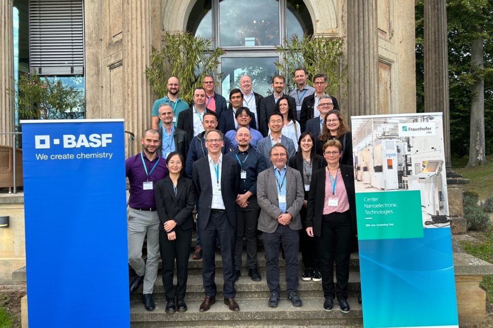
Fraunhofer IPMS and BASF celebrate ten years of collaboration.
More power, more energy-efficiency, more complexity - manufacturers of modern microchips are constantly facing new challenges, also regarding the electrical connections required. Fraunhofer IPMS and BASF have been working together on this problem for ten years. The teams have pooled their infrastructure and expertise and thus have made it possible to evaluate chemicals, processes and product tests for chip integration on an industrial scale.
The Fraunhofer Institute for Photonic Microsystems IPMS and BASF are proud to look back on ten successful years of cooperation. Together, they have been working on innovative and customized solutions in the field of semiconductor production and chip integration as part of their “BASF Plating-Lab”. Within pilot tests at the Center Nanoelectronic Technologies (CNT) of Fraunhofer IPMS, strategies are developed and implemented to make materials and technologies in semiconductor integration more efficient and cost-effective. “With our cooperation, we are addressing the growing challenges in the market and thus enable new technologies in the field of interconnect and packaging”, explains Dr. Lothar Laupichler, Senior Vice President, Electronic Materials at BASF.
Process evaluation according to industry standard
Numerous electro-chemical processes are necessary during the manufacturing and integration of a microchip. Various layers of metal or metal alloys must be applied to the wafer to connect the individual circuits and create the network of conductor paths within a chip. For different steps in the overall integration and different subsequent applications, the chemicals and work steps must be adapted to individual processes of the customers. As part of the collaboration with BASF, new chemicals for electroplating deposition processes have been evaluated in recent years.
At the same time, corresponding product tests and demonstration trials have been carried out for customers at wafer level. BASF installed a state-of-the-art process tool in the clean room at Fraunhofer IPMS, which is operated by Fraunhofer’s experienced scientists. The cooperation partners are thus using the same tools that are applied in the industry processes. This enables customers to significantly reduce their qualification costs. As a result, development time and costs can be saved, and more efficient processes can be established. The innovative solutions can therefore be developed and evaluated directly under production conditions.
Direct application possibilities for industry partners
Over the past ten years, the project partners have achieved over 12,000 process launches. “The chemical packages and products developed can be used directly in our customers’ industrial processes,” says Dr. Benjamin Lilienthal-Uhlig, Head of Business Unit Next Generation Computing at Fraunhofer IPMS. For example, they are used to manufacture wiring structures in miniaturized circuits with dual damascene technology. The products are also important in the manufacturing of interposers, chiplets and 3D packages for rewiring structures (pillar, RDL, TSV) or they might form the metal layers in wafer-to-wafer hybrid bonding.
In June 2014, the research institute and the chemical company established the collaboration as part of the screening fab opened at CNT. Fraunhofer IPMS provides its 300 mm cleanroom infrastructure to BASF for this purpose. Customers and partners also benefit from the Silicon Saxony network, in which the institute is located. It enables the involvement of other local facilities, such as the Dresden branch of Fraunhofer Institute IZM-ASSID, or direct process developments specifically for the global industrial partners of Fraunhofer IPMS (Bosch, Infineon, GlobalFoundries). The newly founded research center CEASAX (“Center for Advanced CMOS and Heterointegration Saxony”) will make it possible to work even closer on application-oriented solutions, especially with regards to the heterointegration of microsystems.


