
High memory bandwidth in the spotlight
A Q and A with Aaron Fellis, corporate vice president and general manager of Wet Equipment Technology Systems at Lam Research.
Q1: This new world of AI requires High Bandwidth Memory (HBM). Why is HBM so critical to the performance of GPUs and, by extension, the advancement of AI?
A1: GPUs are critical to generative AI, but arguably just as critical are the semiconductor innovations that support it — particularly HBM.
GPUs have become the standards for AI training. However, inference from cloud to edge is creating tension between traditional CPU architectures and accelerators as companies try to balance infrastructure performance and efficiency. These solutions share the challenge of feeding huge data sets into incredibly fast processing complexes.
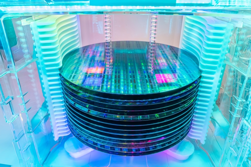
While traditional memory may bottleneck with increasing AI workloads, HBM — a newer form of high-speed memory — provides greater bandwidth and power efficiency to deliver these data sets with near lightning speed. In an HBM chip stack, multiple layers of DRAM chips are vertically integrated, which enables the rapid data exchange needed to perform complex AI tasks. HBM leverages 2.5D and 3D stacking and cutting-edge packaging to deliver improved memory bandwidth while achieving better power efficiency and a smaller footprint than traditional memory alternatives.
Q2: How do 2.5D and 3D stacking and ‘cutting edge’ packaging deliver improved memory bandwidth and higher efficiencies?
A2: Semiconductor breakthroughs, particularly advanced packaging, are enabling the creation of new HBM memory to meet the performance and unique demands of generative AI applications.
Advanced packaging technologies, such as 2.5D and 3D integration, allow for the stacking of memory and logic chips. Stacking relies on through-silicon vias (TSVs) and microbumps. The more TSVs in a chip stack, the higher the interconnect density. This also means data can travel faster and more efficiently.
But as more TSVs are created, their openings get narrower. When this happens, the relative height to that opening (aspect ratio) increases, which makes the electrofill process much more challenging. Proper filling of TSV structures and creation of microbumps is essential to stack HBM chips.
Meanwhile, 2.5D today uses multi-layer submicron metal lines on a silicon interposer to connect multiple dies horizontally and as close possible with minimal routing. These metal lines are formed using fab-based metal damascene processes which include dielectric deposition, etching, cleaning, metal deposition, and, finally, polishing.
Q3: New HBM requires a complex set of manufacturing steps – tell me about this.
A3: HBM has many advantages, but it is not without technical challenges. In the manufacturing of HBM, extremely narrow and tall features must be created with very high precision and repeatability. TSVs, for example, require difficult, multi-step processing. Plasma-based deep silicon etch process tools are used to selectively remove silicon to precisely form uniform, high aspect ratio holes. After cleaning and depositing oxide materials and barrier seed, the microscopic holes are filled through advanced copper electroplating, with care taken that the fill is void-free. At every step, sophisticated tools and equipment play an important role in helping to create consistent and predictable yield.
Lam Research brings expertise in advanced deposition, etch and clean packaging technologies to help chipmakers address manufacturing challenges and ensure that HBM devices meet the stringent performance and reliability standards required by AI applications.
Q4: What are some of the Lam tools and technologies involved in 2.5D and 3D stacking?
A4: Lam provides an industry-leading portfolio of solutions for advanced packaging and 2.5 and 3D stacking. It includes SABRE® 3D, Striker® and Syndion®, which deliver precision and uniformity at the atomic level. These tools are critical enablers of HBM manufacturing and are used by all major memory manufacturers.
•SABRE® 3D electrofill tool is used to metalize TSVs. It fills the etched vias with copper, ensuring solid electrical connections between the stacked layers. This process is crucial for maintaining the performance and reliability of HBM devices.
· Striker® atomic-layer deposition (ALD) delivers an oxide liner that is necessary for TSVs because it helps isolate the copper that is deposited with SABRE 3D. It also reduces process times by using rapid cycles and ALD-rated components, software, and controls.
· Syndion® etch technology uses deep reactive ion etching to deliver a smooth and repeatable profile at a high etch rate. Rapidly alternating process (RAP) — quickly switching between etch and deposition steps during manufacturing — enables the creation of deep, uniform TSVs while protecting sidewalls.
Q5: How are tool vendors, such as Lam Research, developing packaging innovations and collaborating with customers to deliver them?
A5: Leveraging our expertise in etch, deposition and clean processes, Lam continually collaborates with chipmakers to understand their needs and deliver innovative products,
technologies and solutions that address their scaling challenges. We identify the most efficient and cost-optimized way to deliver on a customer’s technical requirements with the fastest processing speed. This allows them to benefit from the most efficient use of capital equipment in their factories and accelerate their abilities to deliver on their HBM product roadmaps.
Q6: We’ve covered quite a lot of ground. If you can, please summarize just how you see this AI opportunity playing out for the semiconductor industry, and Lam Research in particular?
A6: Advanced packaging solutions like HBM are critical approaches for chipmakers to optimize the performance, power, form factor, and cost of their devices. But continuous innovation in chip design and manufacturing processes will be necessary for HBM to propel the AI era. Lam’s expertise and innovations in etch, deposition, and advanced packaging make it well positioned to meet the manufacturing requirements for HBM.


