
DELO introduces UV-approach for fan-out wafer-level packaging
DELO has developed a new approach for fan-out wafer-level packaging (FOWLP).
Its feasibility study shows: With the use of UV-curable molding materials instead of heat curing ones, warpage and die shift can be reduced significantly. Additionally, this leads to improvements in curing time and minimizes the energy consumption.
Both warpage and die shift are typical side effects of fan-out wafer-level packaging, a cost-efficient method in the semiconductor industry where numerous dies are encapsulated together on a carrier. Even though fan-out techniques on wafer- and panel-level constantly get refined, these issues associated with the involved compression molding remain.
Warpage occurs due to chemical shrinkage when the liquid compression mold compound (LCM) cures and cools down after the molding process. The second contribution to warpage is due to the mismatch of coefficient of thermal expansion (CTE) between the silicon dies, mold material and the substrate. Die shift is a result of highly filled, and thus pasty molding materials, which can only be applied under elevated temperature and high pressure. As the dies are mounted on carriers by temporary bonding, increased temperature can soften the temporary adhesive, hence diminishing its function of keeping the chips in place. Simultaneously, the pressure needed to push the molding compound exerts force on each die.
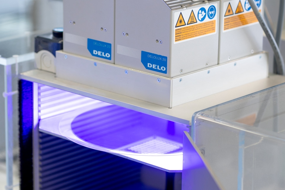
To find a solution for these challenges, DELO conducted a feasibility study, using a simple model of dummy chips bonded to a carrier substrate. For this setup, the carrier wafer was coated with a temporary adhesive and the dies were positioned face-down. Subsequently, the wafer was molded with a low-viscosity DELO material and cured with UV light before the carrier wafer was removed again. Typically, high-viscosity heat-curing molding compounds are used in applications like this.
The experiments, in which DELO also compared the warpage of a heat-curing encapsulant with that of a UV curing product, proved that warpage occurs when typical molding materials cool down after heat curing. Therefore, switching to room temperature curing by using UV light instead of heat significantly reduces the impact of CTE mismatch between the molding compound and carrier, thus minimizing warpage.
With the use of a UV-curing material it is also possible to reduce filler content and, therefore, lower its viscosity and Young’s modulus. In testing, a model adhesive system achieved a viscosity of 35,000 mPa·s and a Young’s modulus of 1 GPa. This leads to minimal die shift as no heat or high pressure is necessary to spread the molding material. Typically used compounds have viscosities of around 800,000 mPa·s and Young’s moduli are in double-digit range.
Overall, the study showed that the utilization of UV-curable large-area molding materials facilitates the production of chip-first fan-out wafer-level packaging wafers with minimal warpage and die shift. Despite the substantial CTE disparity among the materials employed, the process remains versatile due to the lack of temperature variation. Furthermore, UV curing reduces both curing time and energy consumption.
DELO will be at SEMICON Europa in Munich from November 12–15, 2024 to talk about its findings in detail as well as additional bonding solutions for advanced packaging.


