Quantum foundry nears completion

Quantum Computing enters final stage of commissioning quantum photonic chip foundry in Tempe, Arizona.
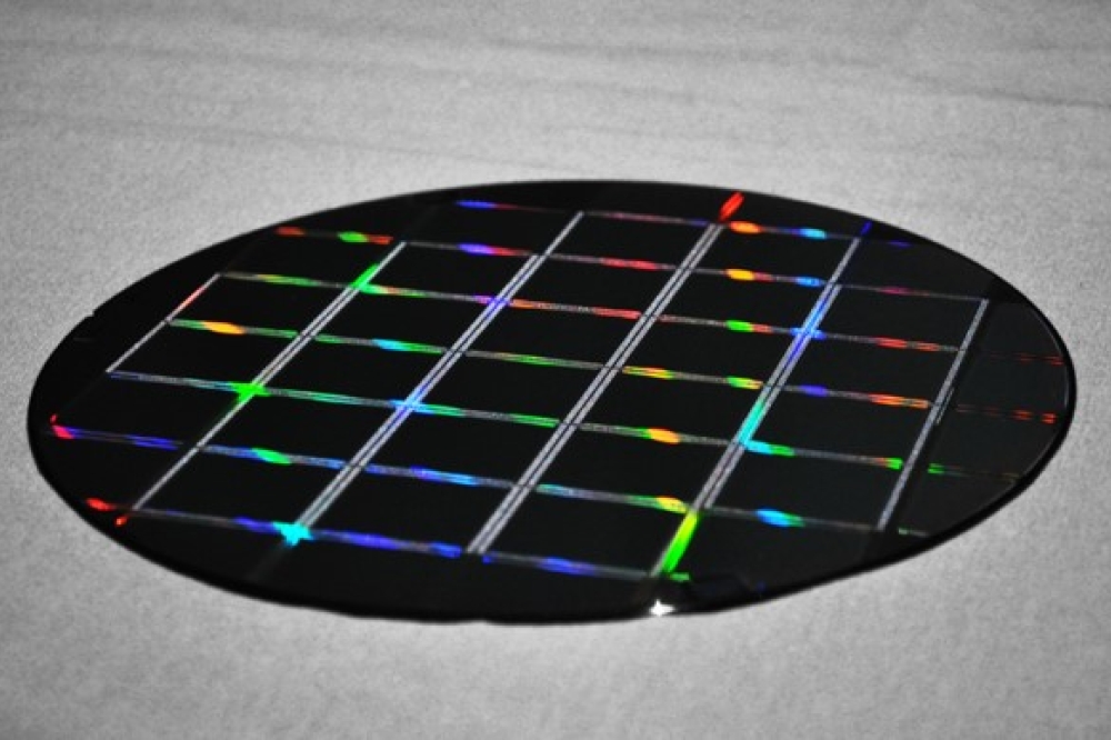
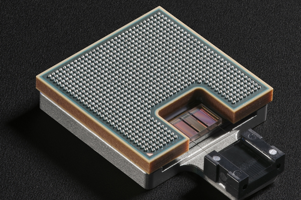
Quantum Computing has reached the final stage of commissioning its quantum photonic chip foundry in Tempe, Arizona. Initially announced in September 2023, the QCi Foundry will focus on processing thin film lithium niobate (TFLN) to produce high-performance optical components and photonic integrated circuits (PICs). These photonic chips will serve as essential optical engines for photonic-based quantum computers, secure quantum communications, and 3.2Tbps data rates for datacom, driven by the increasing demands of artificial intelligence (AI) and enabling the future of integrated photonics.
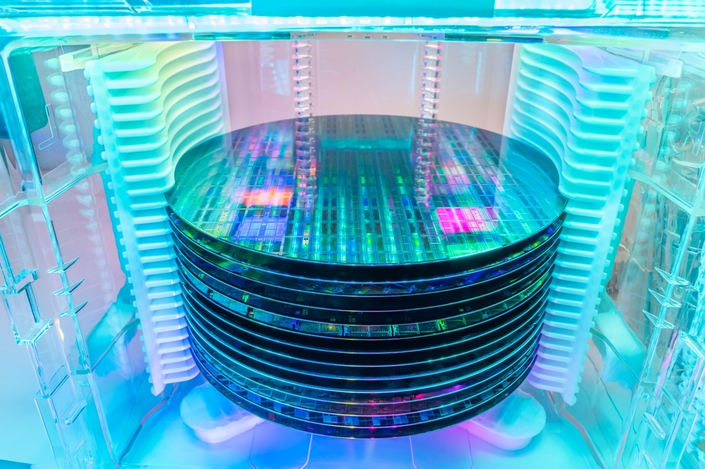
QCi Director of PIC and Foundry Service, Dr. Pouya Dianat, will formally introduce this first-of-its-kind foundry and its services during his presentation at the Optica Photonic-Enabled Cloud Computing (PECC) Industry Summit on October 23, 2024, in Sunnyvale, California. At the summit, Dr. Dianat will discuss how QCi's key technological advantage lies in its precision etching of TFLN, which minimizes the loss of photons in a PIC, alongside wafer-scale production capabilities for TFLN optical components such as electro-optic modulators and waveguides. This commitment ensures successful volume production from early stages of prototyping.
"The QCi Foundry will be the first US-based semiconductor foundry of its kind, set to enhance the capabilities and capacity of TFLN devices. These innovations will also pave the way for advancements and applications in national defense and technology," states Dr. Dianat. "Additionally, the foundry will meet the growing demand and market needs for rapid prototyping and scalable production of photonic integrated circuits. QCi's proprietary TFLN processing technology will provide customers with the agility and confidence necessary for the reliable, seamless integration of TFLN photonic engines into their product lines and offerings."
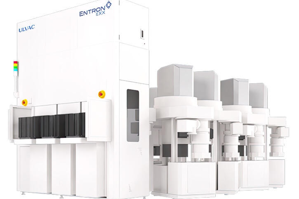
The QCi Foundry has moved into its final phase of construction and capital equipment installation, with an anticipated grand opening set for Q1 2025. As part of its launch strategy, QCi will offer early access to customers and early adopters at favorable rate and terms. The Company's initial wafer runs will focus on custom runs for selected clients, with plans for a multi-project wafer (MPW) run available in the second half of 2025.


