
Wet etch and clean solution with integrated metrology
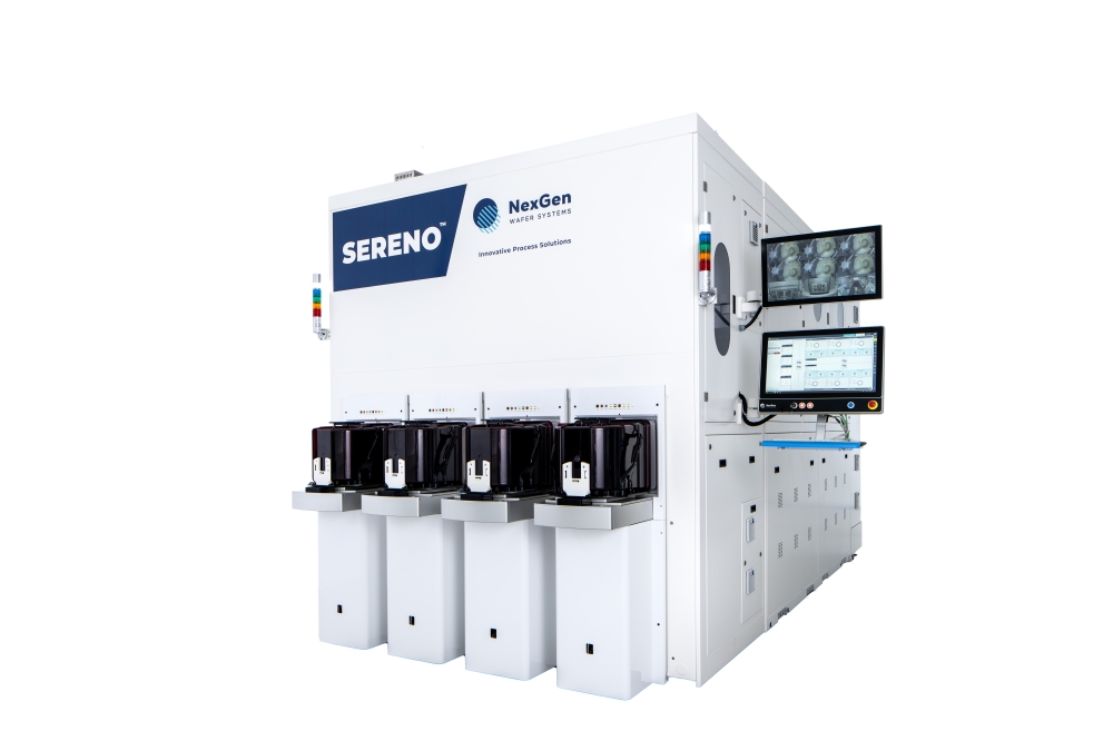
NexGen Wafer Systems has launched SERENO, its latest multi-chamber platform designed for Wet Etch and Clean applications.
SERENO combines high performance with exceptional flexibility, offering integrated metrology for precise substrate and layer thickness control, as well as surface roughness control. Its onboard chemical supply system supports multiple process chemicals with integrated mixing, blending, and comprehensive analytics, ensuring maximum adaptability across a wide range of applications.
With a compact footprint of less than 12 m² and a throughput of up to 200 wafers per hour, SERENO is designed to deliver unmatched efficiency and versatility in wet chemical processes. Tailored for both FEOL and BEOL applications, SERENO addresses the semiconductor industry's increasing demands for higher performance, precision, and cost efficiency, positioning it as a future-proof solution for evolving manufacturing requirements.
Delivering High Performance in a Compact Design
The SERENO platform offers maximum flexibility regarding wafer-handling capabilities and process control. It supports various substrate types for 6", 8” and 12" wafers. Its versatile handling system supports wafer thicknesses ranging from ultra-thin wafers below 100µm to bonded wafers exceeding 2mm in total thickness. High-performance process chambers combined with innovative chemical dispensing and scanning control offer maximum freedom, leading to outstanding on-wafer performance.
“With SERENO, we provide Wet Etch and Clean solutions that deliver high throughput in a compact footprint while maximising the flexibility and performance advantages of Single-Wafer Technology,” said Christian Kleindienst, Chief Marketing Officer at NexGen Wafer Systems. “Our SERENO platform addresses our customers' demand for flexible, high-performance Single-Wafer solutions that reduce operational costs and present a highly attractive alternative to traditional batch tools.”
Key Features of the SERENO Platform
Throughput: Up to 200 wafers per hour
Footprint: ~12m²
Advanced Process Control: Customizable wafer scanning and precise fluid dispensing enable optimal process performance across all dimensions.
Integrated Metrology: Built-in thickness and roughness metrology provide real-time feedback, ensuring process uniformity and quality.
High-Performance Chambers: Industry-leading liquid flow and exhaust performance ensure reliable cross-contamination-free processing.
Versatile Chemical Supply: Onboard storage for up to three process chemicals with dual 90-litre tanks ensures uninterrupted processing.
Flexible Wafer Handling: Supports 6", 8", and 12" wafers, including ultra-thin and fragile substrates, with bridge tool functionality for multiple wafer sizes.
Applications for SERENO Include:
Surface Clean
Particle removal
Polymer removal
Residual removal
Backside/Bevel cleaning
Incoming wafer cleaning
Film and Metal Etch
Backside/Bevel film etch (Silicon Nitride | Silicon Dioxide | Polysilicon)
Metal Etch (Ti | Ni | Ag | Au | Al | W | Cu …)
UBM (Ag | Ni| Ti ...)
Substrate Etch
Thinning
Stress relief
Surface conditioning
Vias reveal
Supported Substrate Types
Si | SiC | GaN | GaAs | Al2O3 | ZnO


