Loading...
News Article

OMNIVISION debuts 'smallest-footprint sensor'
News

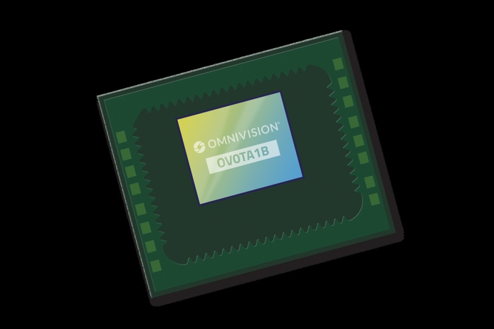
The OV0TA1B sensor is said to be the first and only mono/IR sensor that can fit in 3mm module Y dimension and smaller notebook computers, webcams and IoT devices.

OMNIVISION has introduced the new OV0TA1B monochrome (mono)/infrared (IR) CMOS image sensor, the first and only solution that fits 3mm module Y dimension and smaller notebook computers, webcams and IoT devices. The OV0TA1B is a low-power device that is ideal for artificial intelligence (AI)-based human presence detection (HPD), facial authentication and always-on (AON) technology.


“Stand-alone 940nm IR cameras are becoming more mainstream, especially in the latest generation of ultrathin-bezel design notebooks that feature personalized AI features and require HPD and facial authentication capabilities,” said Jason Chiang, staff marketing manager computing, OMNIVISION. “The OV0TA1B is the newest mono/IR sensor in our computing portfolio designed to be a cost-effective, ultra-small-footprint device; it is ideal for HPD and facial authentication in 3mm module Y bezel and smaller designs. The ultra-small size of the OV0TA1B sensor also makes it useful for webcams and IoT devices, like those used for people and traffic counting.”


The OV0TA1B comes in either IR or mono, depending on the customers’ design needs (in cases where the system has another stand-alone RGB camera). It features a 2-micron (µm) pixel based on PureCel® pixel technology for high-performance sensitivity and MTF (modulation transfer function), allowing it to maintain the HPD and facial authentication.


The OV0TA1B delivers 440 x 360 resolution at 30 frames per second (fps). It is a low-power 220x180 (2.58mW@3fps) image sensor in a 1/15.8-inch optical format.

Silicon photonics market worth $7.52 billion by 2029
MIT team takes a major step toward fully 3D-printed active electronics
Sampling success
Applied Materials and National University of Singapore expand semiconductor research lab
SCI Semiconductors and EPS Global form worldwide distribution agreement
GlobalFoundries and NXP collaborate
Nord Quantique secures semiconductor supply chain
MCUs promise high performance for cost-sensitive applications
OMNIVISION debuts 'smallest-footprint sensor'
Research for the future, application transfer for the present
EnSilica strengthens partnership with TSMC
esmo group launches Apollo Quad Handler
Mycronic receives order for two SLX mask writers
Tenstorrent expands deployment of Arteris’ Network-on-Chip IP
Wet etch and clean solution with integrated metrology
James Culp of GlobalFoundries joins Si2 Board
Infineon presents new ASIL-D-compliant 3-phase gate driver IC
JST names Dr. Ismail Kashkoush as Chief Technology Officer
DuPont earns Best Partner Award for Innovation from Samsung Electronics
Advantest to showcase latest semiconductor test solutions
Infineon introduces DEEPCRAFT brand for Edge AI software solutions
Ohio State University selects Veeco system
Global Wafer Fab Equipment revenue poised to surge
New educational initiative for the German chip industry
ZEISS launches Crossbeam 550 Samplefab FIB-SEM
Critical Manufacturing brings highly advanced MES solution to SEMICON Europa
Infineon at electronica 2024: Solutions for decarbonisation and digitalisation
Infineon unveils "world’s thinnest" silicon power wafer
Sunlit Chemical expands global reach with US facility opening in Phoenix
Semiconductor patent applications up 22% globally to 81,000 a year
Promoting collaboration and novel IC design technologies
EV Group announces board expansion In light of unabated growth
×
Search the news archive

To close this popup you can press escape or click the close icon.
Logo
x
Logo
×
Register - Step 1

You may choose to subscribe to the Silicon Semiconductor Magazine, the Silicon Semiconductor Newsletter, or both. You may also request additional information if required, before submitting your application.


Please subscribe me to:


You chose the industry type of "Other"

Please enter the industry that you work in: