Research for the future, application transfer for the present
Advancements in industry and technology are constantly demanding new solutions for the manufacturing of microchips regarding the technical, economic and also ecological perspective.
The Fraunhofer Institute for Photonic Microsystems IPMS has established itself as a strong partner to industry with its pioneering research and state-of-the-art equipment. The range of services includes all steps “from lab to fab” - from consulting and process development to pilot production.
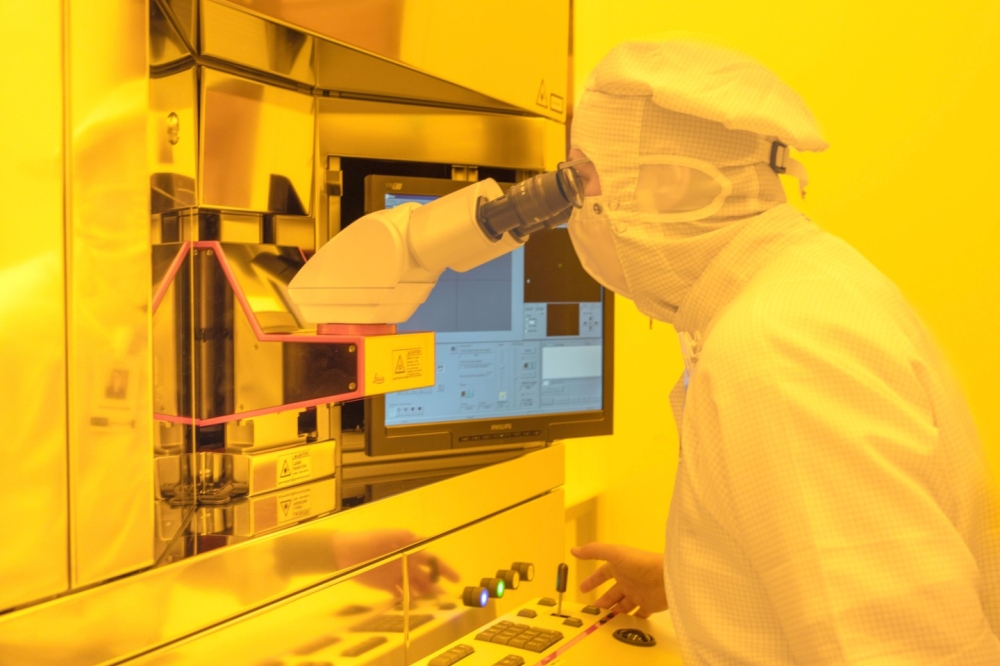
Lithography in the 300-mm-clean-room at Fraunhofer IPMS - Center Nanoelectronic Technologies (CNT).
While systems and components have to meet ever higher performance requirements, it is also essential that they are compatible with further industrial processes in the semiconductor industry and comply with the latest technology standards. Easy and fast integration, a wide range of applications and cost efficiency are key parameters. Fraunhofer IPMS is working on innovative solutions in the field of memory technologies, sensors and actuators as well as MEMS systems. With its comprehensive range of services and intensive cooperation with chip manufacturers, system manufacturers and suppliers the institute enables the rapid transfer of results and technologies.
New computing architectures and innovative storage for the next generation of computers
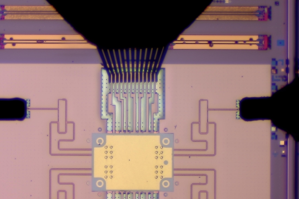
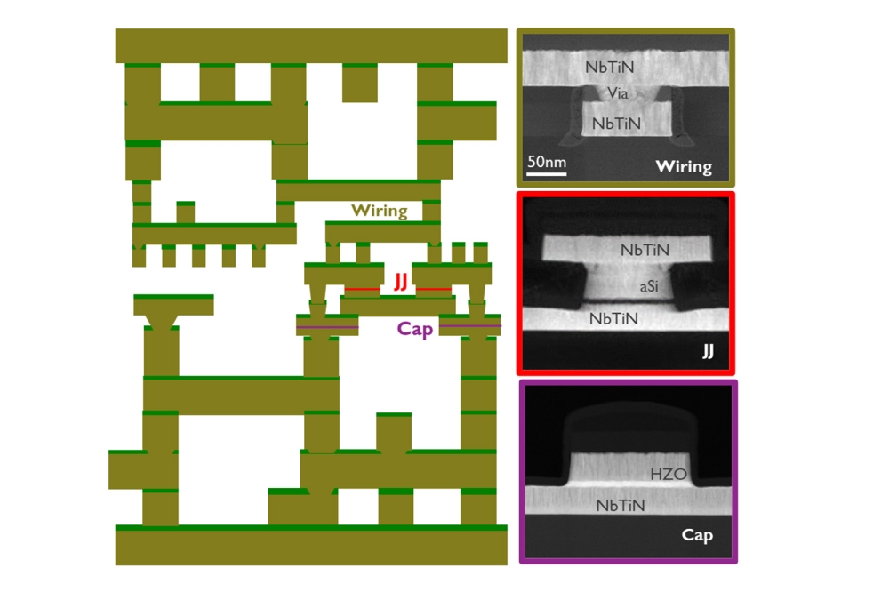
We generate a growing amount of data every day. To deal with this, new technologies are required that enable this information to be stored and processed quickly. With this in mind, Fraunhofer IPMS is researching the next generation of computers. In projects with international partners, such as “QSolid”, “Qu-Pilot” or “QUASAR”, the institute is working on the production of qubits and the construction and architecture of quantum computers. The research focuses on industry-oriented scalability of electronics, optimized materials, processes and control technologies in regard to their CMOS compatibility.
Non-volatile memory (NVM) solutions are becoming increasingly important for modern data processing, as they are more powerful, cost-effective and energy-efficient. Fraunhofer IPMS can look back on more than ten years of experience in the development of MRAM, RRAM and ferroelectric technologies. Of particular note are hafnium oxide-based ferroelectric memories, which can be seamlessly integrated into advanced CMOS technologies, offering significantly better performance and lower cost. Another promising energy-saving while high-performance technology is In-Memory-Computing. Here, data is processed directly at the point of origin, i. e. in the memory arrays.
The research services of Fraunhofer IPMS in this area include the development of system designs, circuit designs and integration concepts, as well as material research and characterization up to the megabyte range. With the implementation of materials into production lines using wafer loops, a direct transfer into existing technology nodes can be guaranteed.
Application-oriented MEMS, MOEMS and Microdisplays on 200-mm silicon wafers
In two ultra-modern 200-mm clean rooms, Fraunhofer IPMS develops MEMS, MOEMS and microdisplay technologies along the entire value chain: from individual processes and technology modules to pilot production and support for technology transfer as well as licensing. The institute thus covers the technological maturity levels from 3 to 7. Start-ups, SMEs and companies without their own fabs benefit from low investment costs thanks to the full-service offering. To make it easy for SMEs in particular to get started, the institute also offers evaluation kits for all of its developments, which are ready-to-use set-ups that customers can employ to test the Fraunhofer IPMS technologies directly in their own application.
The institute further develops innovative components such as sensors, actuators and microdisplays in their 200-mm-clean-rooms. The latter recently achieved a new world record of 45% transparency. The microdisplays are ideal for virtual reality, augmented reality and mixed reality applications in industrial production or medical technology due to their very high resolution and technological level.
Close links with the semiconductor industry
To accelerate the transition from laboratory to practical application, Fraunhofer IPMS offers a strong network and close cooperation with industry. At the same time, this promotes Germany's technological competitiveness. The institute recently celebrated 10 years of collaboration with BASF in the field of new materials for microchips. GlobalFoundries has also been a close partner in process development for many years, just like Bosch. The long-standing partnership with Bosch focuses on the development of MEMS technology, for example in the development of micro loudspeakers. Furthermore, the institute operates a metrology center with Applied Materials. In the Screening Fab at the Center Nanoelectronic Technologies (CNT), materials, processes and machines can be evaluated under industrial conditions, in accordance with the ISO 9001 standard and at ultra-large-scale integration level (ULSI).
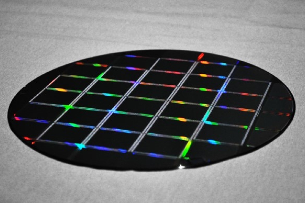
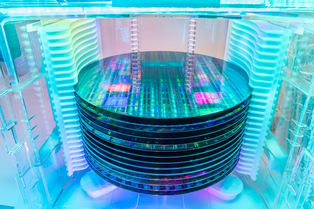
Customers, chip and equipment manufacturers, suppliers and other R&D partners also have access to services on 200-mm and 300-mm wafers. The services range from atomic layer deposition, chemical-mechanical polishing, wafer metallization and wafer cleaning to metrology and nanopatterning.
Increasing importance of sustainability
Sustainable microelectronics is increasingly becoming the focus of modern developments in order to address ecological challenges in the industry. By using resource-saving materials and energy-efficient manufacturing processes, the carbon footprint can be minimized. Fraunhofer IPMS is involved in a number of projects, including the “Green ICT @ FMD” competence center of the Research Fab Microelectronics Germany. The main aim is to find and evaluate alternative and more environmentally friendly materials or processes and to significantly reduce energy and material consumption during production. With this, future-proof microelectronics can be developed, that meet the requirements of sustainability and at the same time strengthen technological competitiveness.
Bundled expertise at Semicon Europa
Fraunhofer IPMS will be presenting its latest research results and technical possibilities at “Semicon Europa” from November 12 to 15 in Munich. Visitors will have the opportunity to get in touch with the researchers at the joint Silicon Saxony stand in Hall C1 #419/33. Appointments can be made in advance via the Fraunhofer IPMS website. At the stand, they can also talk to experts from Fraunhofer ENAS, Fraunhofer IZM-ASSID and the Leibniz Institute for Innovative Microelectronics (IHP) - all of which are part of the Research Fab Microelectronics Germany (FMD).


