Applied Materials and National University of Singapore expand semiconductor research lab
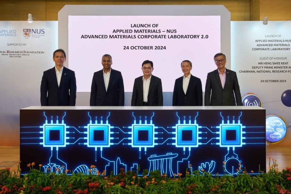
New phase will include larger, more advanced cleanroom, establishment of a Professorship at NUS, and new programmes for talent development.
Applied Materials South East Asia Pte. Ltd. and the National University of Singapore (NUS) are furthering their collaboration to bring advanced semiconductor research capabilities and talent development opportunities to Singapore. Supported by the National Research Foundation (NRF) under the Research, Innovation and Enterprise 2025 (RIE2025) plan, the Applied Materials-NUS Advanced Materials Corporate Lab – established in 2018 and located on the NUS Kent Ridge campus – will be expanded with state-of-the-art semiconductor process equipment in a larger, more advanced cleanroom. In addition, Applied Materials and NUS are collaborating on programmes designed to strengthen Singapore’s talent pipeline.
Mr Heng Swee Keat, Deputy Prime Minister and Chairman of NRF, was the Guest-of-Honour at a ceremony held recently at NUS marking the new phase of the Corporate Lab. Guests from the industry, local research ecosystem and government agencies attended the event.
“When NUS and Applied Materials first established the Corporate Lab six years ago, we laid the foundation for a collaboration that has since yielded remarkable success,” said NUS President Professor Tan Eng Chye. “Several of the innovations developed here have progressed from the research stage to the scale-up phase, paving the way for real-world applications that can benefit society. We are very excited to embark on a new chapter in our collaboration with Applied Materials to further advance semiconductor science and technology and inspire the next generation of innovators who will push the envelope and break new ground in this significant field.”
“The Advanced Materials Corporate Lab at NUS is a prime example of how industry-academia collaboration can accelerate the discovery and transition of innovations into commercial applications,” said Dr Satheesh Kuppurao, Group Vice President of Business Development and Growth, Semiconductor Products Group at Applied Materials, Inc. “Our joint work has resulted in numerous patents related to chemistry, semiconductor process and hardware design solutions, along with several sponsored scholarships. Applied Materials is excited to build on our success with NUS and bring enhanced semiconductor research and talent development opportunities to Singapore.”
Hosted at the College of Design and Engineering and the Faculty of Science at NUS, the Applied Materials-NUS Advanced Materials Corporate Lab offers world-class, multi-disciplinary R&D capabilities that span applied chemistry, materials science and microelectronics process engineering. The goal of the Corporate Lab is to accelerate discovery of new materials that can be quickly transferred into commercial applications for manufacturing future generations of semiconductors.
The second phase of the Corporate Lab will elevate the well-established microelectronics research capabilities at NUS to new heights by fostering innovation, accelerating the development of cutting-edge technologies and expanding interdisciplinary collaboration. It will include a new cleanroom in NUS with state-of-the-art materials synthesis and characterisation capabilities. Utilising these enhanced capabilities, Applied Materials and NUS will focus on developing industry-scale solutions to complex semiconductor manufacturing challenges, with an emphasis on integrated processes and interface engineering.
Along with the new phase of the Corporate Lab, the Applied Materials Professorship has been established at NUS to attract experts in semiconductors, materials science and other technology fields. In addition, the enhanced capabilities at the Corporate Lab will introduce new educational and talent development opportunities for undergraduates, postgraduates and professionals in the areas of microelectronics, advanced materials and process engineering. This will ensure the University’s sustained academic leadership within these critical fields and contribute to Singapore’s overall economic growth and development.
For Applied Materials, the latest phase of its collaboration with NUS is part of the company’s “Singapore 2030” plan to strengthen its manufacturing capacity, R&D capabilities, technology ecosystem partnerships and workforce development in Singapore.


