Q.ANT launches commercial photonic processor

Available Now: Q.ANT's first Native Processing Unit is poised to provide at least 30x energy efficiency improvements and substantial performance boost bringing data centre sustainability within reach.
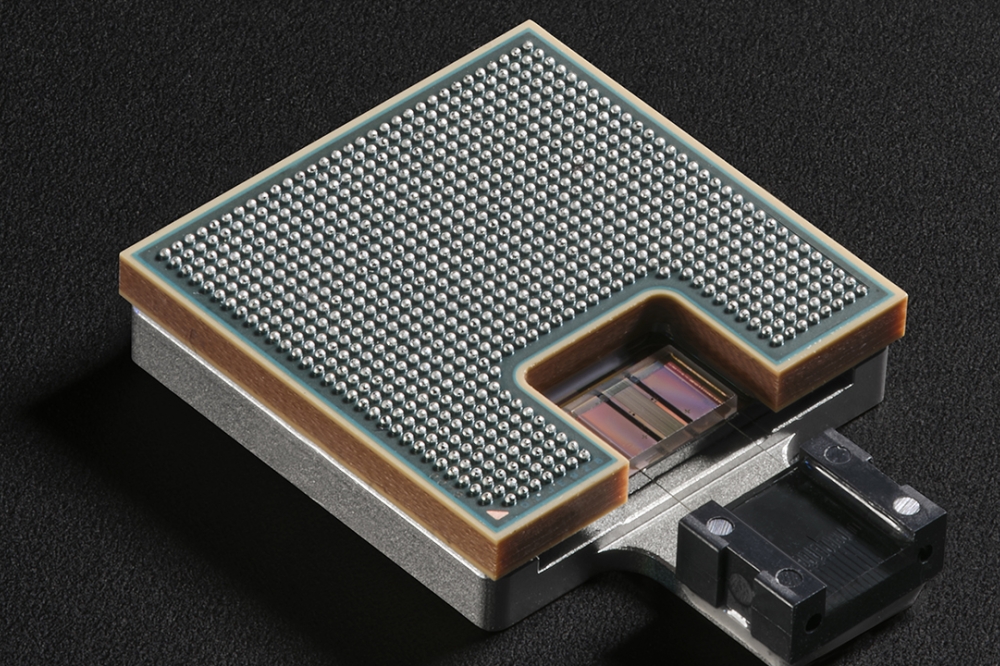
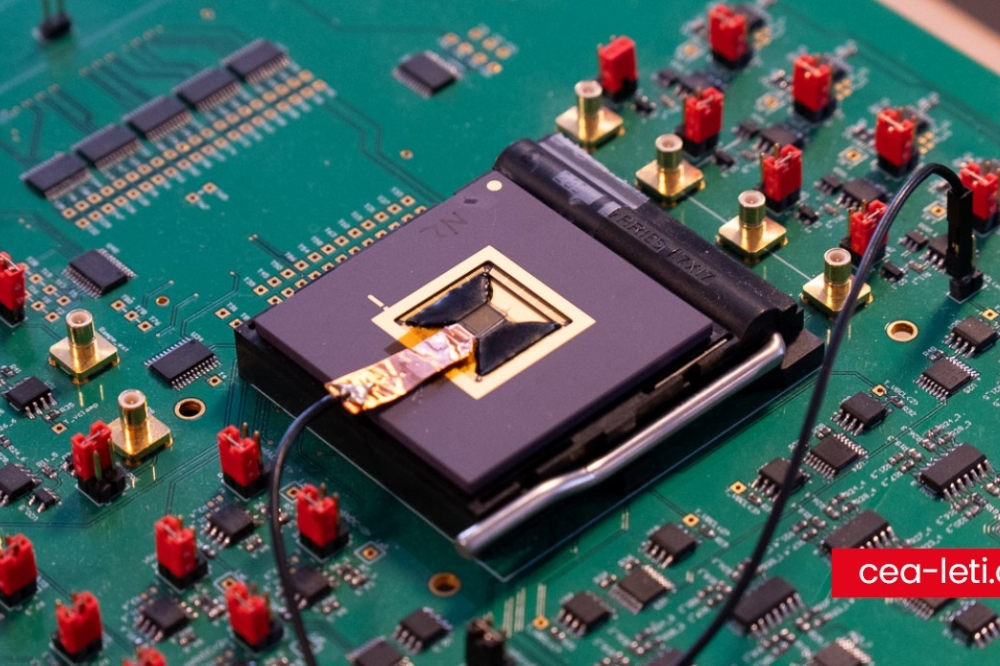
Q.ANT, the leading startup for photonic computing, has launched its first commercial product – a photonics-based Native Processing Unit (NPU) built on the company’s compute architecture LENA - Light Empowered Native Arithmetics. The product is fully compatible with today’s existing computing ecosystem as it comes on the industry-standard PCI-Express. The Q.ANT NPU executes complex, non-linear mathematics natively using light instead of electrons, promising to deliver at least 30 times greater energy efficiency and significant computational speed improvements over traditional CMOS technology. Designed for compute-intensive applications such as AI Inference, machine learning, and physics simulation, the Q.ANT NPU has been proven to solve real-world challenges, including number recognition for deep neural network inference
"With our photonic chip technology now available on the standard PCIe interface, we’re bringing the incredible power of photonics directly into real-world applications. For us, this is not just a processor—it's a statement of intent: Sustainability and performance can go hand in hand,” said Dr. Michael Förtsch, CEO of Q.ANT. “For the first time, developers can create AI applications and explore the capabilities of photonic computing, particularly for complex, nonlinear calculations. For example, experts calculated that one GPT-4 query today uses 10 times more electricity than a regular internet search request. Our photonic computing chips offer the potential to reduce the energy consumption for that query by a factor of 30."
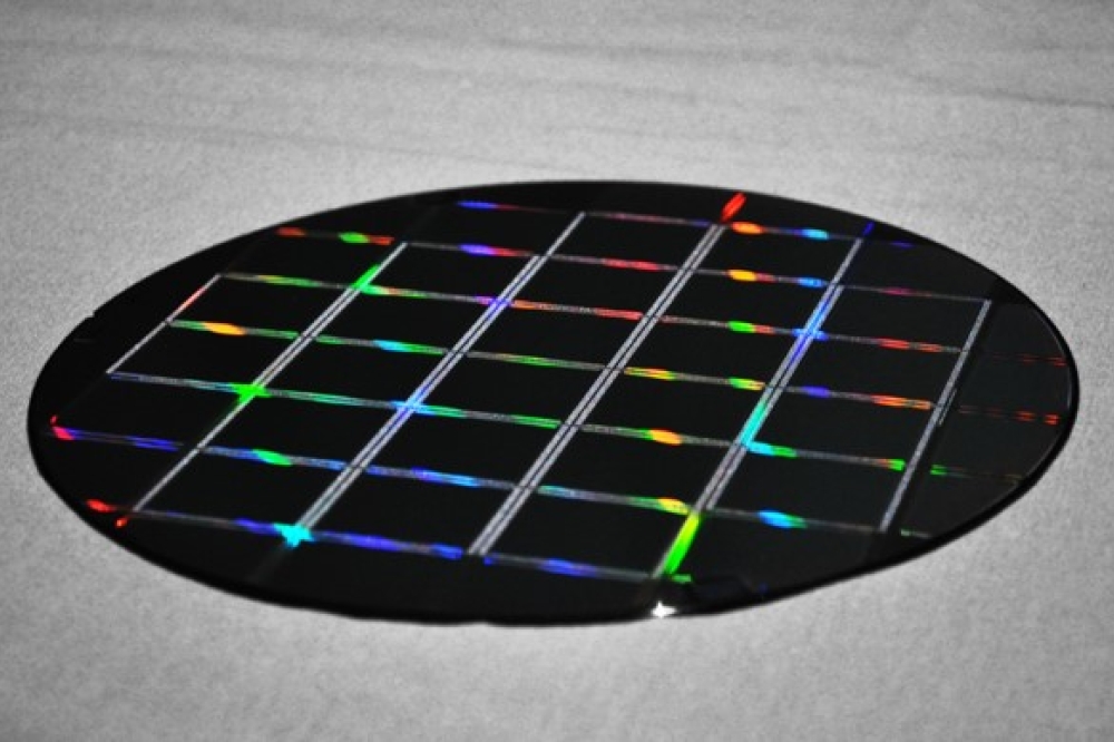
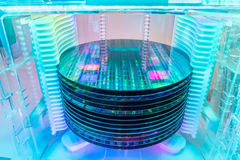
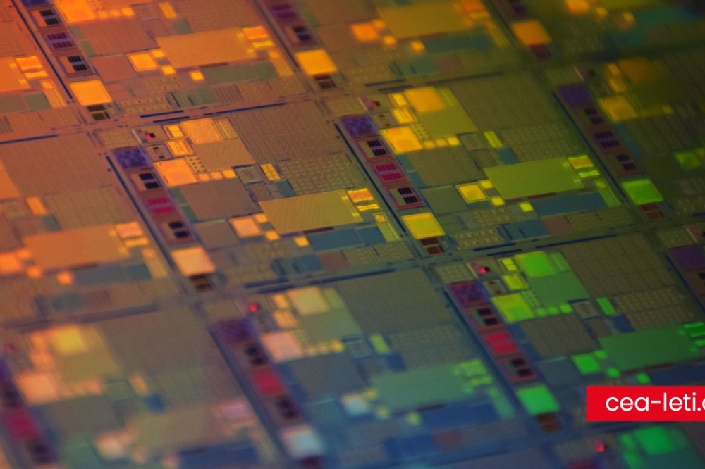
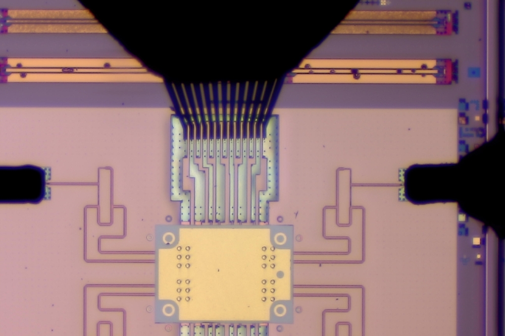
Q.ANT's breakthrough relies on its proprietary LENA platform, which includes Thin-Film Lithium Niobate (TFLN) on Insulator chips. Q.ANT has been developing this photonic material since its foundation in 2018. This platform enables precise light control at the chip level. By controlling the entire value chain from wafer to finished processors and leveraging its deep understanding of light, Q.ANT achieves mathematical and algorithmic density surpassing conventional CMOS technology. For instance, a Fourier transform that requires millions of transistors in traditional computing can be accomplished with a single optical element.
“Q.ANT’s novel approach to photonic processing is a groundbreaking step towards addressing the escalating energy demands of the AI era,“ said Eric Mounier, PhD. Chief Analyst, Photonics & Sensing at Yole Group. “This breakthrough is made possible by using optimal materials for optical circuits, which Q.ANT has engineered over the last few years. This new processor generation finally gives access to superior mathematical operations, which have been too energy-demanding on traditional GPUs. The first impact is expected in AI inference and training performance, paving the way for high-efficiency, sustainable AI computing.” (Source: Optical Computing report, Yole Intelligence, 2024)
The Q.ANT NPU is poised to reduce the calculation requirements for machine learning applications in computer vision or the training and inference of large language models (LLMs.):
● Test runs of the Q.ANT NPU demo system in the cloud with MNIST datasets showed that Q.ANT's native computing approach achieves accuracy comparable to linear networks with lower power consumption.
● Simulations of Kolmogorov-Arnold-Networks (KAN) showed that 43% fewer parameters are required and the number of operations can be reduced by 46%, establishing it as a more efficient choice for AI inference.
● Further tests and simulations on image recognition show that the Q.ANT NPU can train significantly faster and achieve accurate recognition with only 0.1 million parameters and 0.2 million operations. A conventional approach struggles to achieve acceptable results even with 5.1 million parameters and 10 million operations.
Furthermore, it enables faster solutions for partial differential equations in physics simulations, simplifies time series analysis, and improves efficiency in solving graph problems. Unlike standard CMOS technology, the Q.ANT NPU processes data via light, allowing for more power-efficient mathematical operations. While a conventional CMOS multiplier requires 1,200 transistors to perform a simple 8-bit multiplication, the Q.ANT NPU achieves this with a single optical element.


