AlixLabs awarded 345,000€
Funds awarded from Swedish innovation agency’s “Acceleration of deep tech companies 2024” call.
AlixLabs AB, a Swedish startup pioneering advanced semiconductor solutions, has been granted 4 MSEK in funding from Swedish innovation agency Vinnova, equivalent to approximately 345,000 EUR. The funding is spread out over three years with 658,000 SEK (~56,000 EUR) credited immediately, with the remainder to follow over the coming three years. The funds will help AlixLabs’ further its APS™ technology to a higher Technology Readiness Level (TRL) and strengthen customer engagement efforts.
The funding is part of Vinnova’s initiative to accelerate deep tech companies, recognizing the potential of AlixLabs’ APS™ technology to enable cost-efficient Ångström-level scaling for the semiconductor industry.
“We are always pleased to receive recognition and state support for our efforts to scale up our business and commercialize our technology,” said Amin Karimi, COO and R&D Manager at AlixLabs. “The support comes at a crucial stage as we are installing our first 300-millimeter tool in our clean room and are increasingly engaging with potential clients around the semiconductor industry. At the core of our efforts is our APS™ technology which we are convinced is the most sustainable and affordable way forward for semiconductor manufacturing at 3 and 2 nanometers and beyond.”
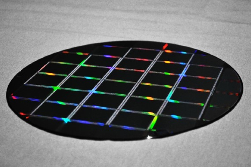
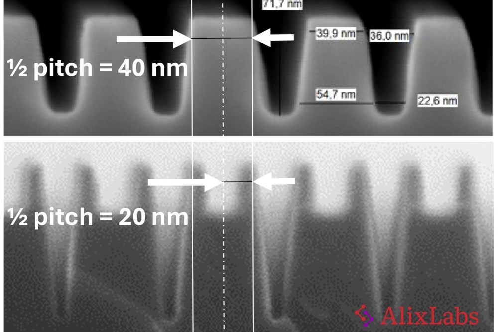
AlixLabs’ offering includes its APS™ technology (Atomic Layer Etch Pitch Splitting) that already allows for etching of feature sizes comparable to those of today’s 3-nanometer class chips with the company’s own equipment. With other proprietary ALE (Atomic Layer Etching) processes, AlixLabs can also contribute to RF and Power IC Gallium Nitride (GaN) and Silicon Carbide (SiC) workflows, with pattern transfer, precision etching and surface roughness reduction for wafers.
“The semiconductor industry is facing a big challenge with regards to sustainability and rising costs to manufacture leading-edge semiconductors. We propose etching instead of costly EUV lithography, and our demonstrations show that we can help produce sub-3-nanometer chips at 35–50 percent lower costs per wafer pass than by using EUV,” said Jonas Sundqvist, CEO at AlixLabs. “While we target the leading-edge logic and memory producers with APS™, our technology also makes it possible for foundries who have given up pursuing sub-20-nanometer production to scale down in a cost-effective way.”
The Vinnova grant will be used by AlixLabs to accelerate the commercialization of its APS™ technology by deepening customer engagement and conducting demonstration projects. These demos will be carried out both at AlixLabs’ facilities and on customer platforms, showcasing the practical advantages of APS™. This approach is expected to advance the Technology Readiness Level (TRL) of our solutions, paving the way for broader industry adoption and reinforcing AlixLabs’ commitment to delivering innovative, cost-effective scaling solutions for semiconductor manufacturing.


