Flash in space
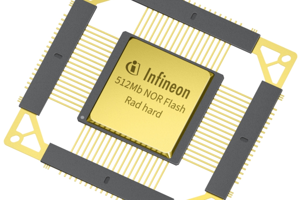
Infineon delivers what it says is the industry’s first radiation-hardened-by-design 512 Mbit QML-qualified NOR Flash for space industry applications.
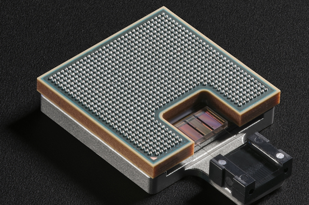
Infineon Technologies has introduced the industry’s first radiation-hardened-by-design 512 Mbit QSPI NOR Flash memory for space and extreme environment applications. The new device offers a fast quad serial peripheral interface (133 MHz) and the highest density, radiation, and single-event effects (SEE) performance available in a fully QML-qualified non-volatile memory for use with space-grade FPGAs and microprocessors.
The new device, which was funded in part by the U.S. Air Force Research Laboratory, Space Vehicles Directorate (AFRL) and jointly developed with Microelectronics Research Development Corporation (Micro-RDC), is based on Infineon’s field-proven SONOS (Silicon-Oxide Nitride-Oxide-Silicon) charge gate trap technology and operates at speeds up to 30 percent faster than lower density alternatives.
“Designers of next-generation space-grade systems continue to demand high-reliability, high-density memories. Working with such industry-leaders as Infineon and Micro-RDC led to a technology solution that combines high density and fast data rates with superior radiation performance compared to alternatives,” said Richard Marquez, AFRL Space Electronics Technology Program Manager.
“Infineon’s radiation-hardened-by-design NOR flash memory is an ideal complement to Micro-RDC’s family of solutions for extreme application environments,” said Joseph Cuchiaro, President, Micro-RDC. “With the availability of 512 Mbit density devices, designers will be able to implement systems with the performance to meet stringent requirements across a wider range of mission profiles than previously possible.”
“The extension of Infineon’s 512 Mbit NOR Flash memory to its rad-hard memory portfolio is further testament to our commitment to deliver highly reliable and high-performance memories for next-generation space requirements,” said Helmut Puchner, Vice President, Fellow, Aerospace and Defense, Infineon Technologies. “This collaborative effort with AFRL and Micro-RDC advances the industry state-of-the-art to address the extreme environments encountered in space applications with technology that will improve performance in critical satellite functions.”
Infineon’s SONOS technology underlies a unique combination of density and speed, as well as unsurpassed radiation performance, with excellent endurance of up to 10,000 P/E and up to 10 years of data retention. The 133 MHz QSPI interface provides fast data transfer rates for space-grade FPGA and processors. A ceramic QFP (QML-V) package occupies 1” x 1” board area, and an even smaller footprint plastic TQFP (QML-P) 0.5” x 0.8” is available. Additionally, the device offers the highest density TID/SEE performance combination for space FPGA boot code solutions and the QML-V/P with DLAM certification meets the most stringent industry qualifications.
A typical use case for this device includes configuration image storage for space-grade FPGAs and standalone boot code storage for space grade multi-core processors.


