3D Semiconductor Packaging market to achieve USD 57.19 bn by 2034
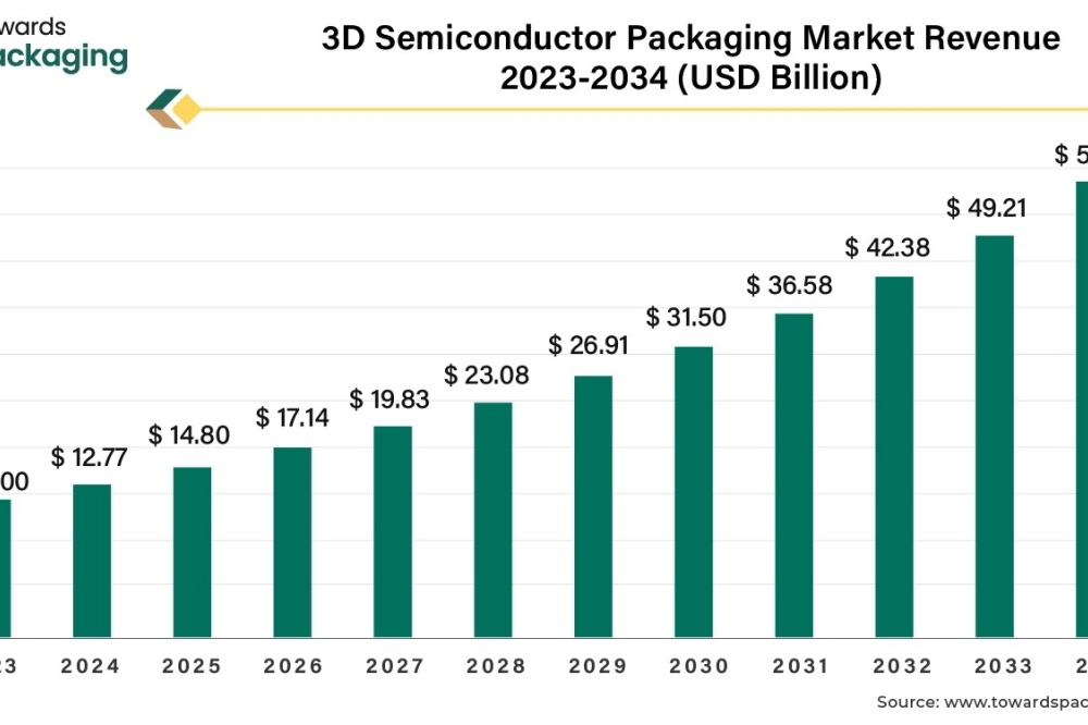
The global 3D semiconductor packaging market size reached USD 12.77 billion in 2024 and is projected to hit USD 57.19 billion by 2034, increasing at CAGR of 16.17% between 2024 and 2034.
The global 3D semiconductor packaging market size is expected to surge from USD 14.80 billion in 2025 to USD 57.19 billion by 2034, a study published by Towards Packaging a sister firm of Precedence Statistics. The market is projected to grow at a double-digit CAGR of 16.17% during the forecast period.
The Evolution of 3D Semiconductor Packaging: Market Overview
The 3D semiconductor packaging market is growing rapidly, as semiconductors are particularly important for small, high performance electronic devices, such as smartphones, tablets, and wearables. 3D semiconductor packaging increases device efficiency. Semiconductor packaging technology has evolved from the original 1D PCB level to the cutting-edge 3D hybrid bonding packaging at the chip level.
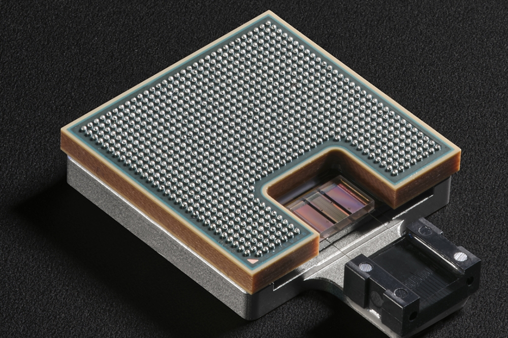
This advancement facilitates single-micron interconnect spacing, enabling bandwidths greater than 1000 GB/s and high performance. 3D semiconductor packaging enables multiple semiconductor chips to be encased into a single package. This packaging shields the integrated circuit and ensures thermal management.
The increasing trend of miniaturization in electronic devices is propelling the growth of the market. As the production of electronic devices increased, 3D packaging has become a mainstream technology for combining multiple dies into a single package and offers many advantages over 2D packaging. Various techniques like the flip chip, wire bonding, ball grid array, and wafer-level packaging are used according to industry requirements. Semiconductor packaging further reduces heat dissipation.
Apart from this, the rising demand for advanced packaging solutions for high-end applications and the availability of cost-effective materials also contribute to the growth of the market. However, high-end devices often require high-quality and durable packaging.
With technological advancements, the 3D semiconductor packaging market is expanding rapidly. This method stacks several semiconductor chips in a three-dimensional configuration and provides a range of benefits, including efficiency, reduced package size, improved power efficiency, and better thermal performance. Fewer interconnects and a compact design further optimize device functionality
Get the latest insights on packaging industry segmentation with our Annual Membership: https://www.towardspackaging.com/get-an-annual-membership
Market Trends
• Growing demand for electronics: 3D semiconductor packaging reduces the overall size of electronic devices by stacking components. Due to shorter interconnects, 3D semiconductor packaging decreases latency, improves bandwidth, and reduces power consumption. It also enhances performance, thermal management, and power efficiency.
• Need for advanced packaging solutions: Due to the rising need for packaging multiple chips in a single package, the demand for advanced packaging is rising. This packaging can perform better in applications like generative AI, automotive computing, and mobile devices. The single package also reduces manufacturing costs and energy consumption. The rising focus on adapting to greater complexity also boosts the market. The transition from a single chip to a whole system design encourages chip designers to adopt advanced packaging solutions.
• Demand for high-performance computing: 3D packaging is suitable for high-performance applications, such as cloud computing, data centers, and gaming. 3D packaging further reduces the interconnect length, reducing signal delay and power consumption.
Insights from Key Regions
Rising production and adoption of electronic devices to support Asia Pacific’s dominance
In 2023, Asia Pacific led the 3D semiconductor packaging market. There is a high demand for consumer electronics in the region, which is a major factor contributing to its dominance. With the rising production of electronic devices, manufacturers increasingly demand 3D semiconductor packaging, as semiconductors are a major component used to develop electronic devices.
This further encourages regional market players to come up with new packaging designs. Countries like China, Japan, South Korea, and Taiwan are the leading contributors to the market. Countries like China, Japan, and South Korea are major manufacturing hubs. Moreover, rising urbanization and industrialization and the rapid expansion of the electronics industry further contributed to regional market growth.
North America is the fastest-growing market
Due to rising technological innovations, North America is the fastest-growing region in the 3D semiconductor packaging market. The region also has a high demand for smart electronic devices. Key players in the region are investing in the research and development of sustainable packaging solutions due to its strong focus on sustainability. Moreover, the rising production of automobiles and government support for the domestic semiconductor industry further contribute to regional market growth.
According to a report published by the U.S. Department of Commerce in November 2024, the Biden-Harris administration announced the CHIPS incentives award with TSMC Arizona to secure U.S. leadership in advanced semiconductor technology.
Future of the 3D Semiconductor Packaging Market
Advancements in 3D Packaging Technology
Utilizing technologies like artificial intelligence (AI) and machine learning (ML) in the packaging process greatly helps to automate the entire process. AI and ML can analyze data and monitor the process, further eliminating human errors and enhancing operational efficiency. The development of 3D packaging technology is occurring in three distinct phases, each leading to the development of next-generation electronic products.
The first phase focuses on die stacking to improve performance and integration. In contrast, the second phase introduces the integration of silicon vias (TSVs) for in-die interconnects to advance miniaturization and joint ventures. The focus of the current phase has shifted to 3D heterogeneous integration.
With innovations in microbump bonding technology and the advancement of TSVs that improve the interconnection between inter-chip, 3D heterogeneous integration has become a major driver of integration from chip fabrication to system level. This advancement not only addresses the growing need for better performance but also creates significant opportunities in the 3D semiconductor packaging market.
• In June 2024, Rapidus Corporation, an advanced logic semiconductor manufacturer, and IBM, a multinational technology company, announced a partnership to develop production technologies for chiplet packages. Rapidus will have access to IBM’s best-in-class semiconductor packaging technology through this partnership.
3D Semiconductor Packaging Market Segment
By technology, the 3D through silicon via segment dominated the market in 2023. This is mainly due to its improved performance and lower power consumption. This technology enables different types of chips to be integrated within a single package. 3D TSV technology improves thermal conduction between chips and allows for better heat management in densely packed configurations, which is crucial for maintaining performance and reliability.
By material, the organic substrate segment led the market in 2023. This is primarily due to its properties, such as flexibility and lightweight. The organic substrate provides mechanical and environmental protection and can also work as a conductive interconnector between semiconductors and PCBs.
On the other hand, the bonding wire segment is expected to expand at the fastest rate in the coming years. It provides a strong bond between the wire and substrate and interconnects between an IC on a silicon die and its packaging. Moreover, its high usage in electronic devices due to its low cost further contributes to segmental growth.
By industry vertical, the automotive & transport segment registered its dominance in 2023. This is mainly due to a significant rise in vehicle production. Semiconductors are widely used in ADAS technologies, which enhances vehicle safety and automation.
Competitive Landscape
Key players competing in the market are International Business Machines Corportation, Suss Microtec AG, Intel Corporation, Taiwan Semiconductor Manufacturing Company Ltd., ASE Group, and Siliconware Precision Industries. These market players adopt various strategies to gain a competitive edge.
Taiwan Semiconductor Manufacturing Company Ltd. Continues to focus on 3D semiconductor packaging with its recent partnership with Amkor Technology, Inc. The two companies have signed a memorandum of understanding to collaborate and bring advanced packaging and test capabilities to Arizona, further expanding the region’s semiconductor ecosystem.
3D Semiconductor Packaging Market Companies
• International Business Machines Corporation (IBM)
• Suss Microtec AG
• Intel Corporation
• Taiwan Semiconductor Manufacturing Company Ltd. (TSMC)
• ASE Group
• Siliconware Precision Industries
Recent Developments in the Market
• In November 2024, Lightmatter announced its partnership with Amkor Technology, Inc., a leader in semiconductor packaging and test services, to create the world’s first largest 3D-packaged chip complex utilizing Lightmatter’s innovative Passage platform.
• In 2023, Samsung announced plans to develop three-dimensional (3D) chip packaging technology that can combine memory and processors to fine-tune chips in small sizes.
More Insights in Towards Packaging:
• The global laminated can packaging market size reached US$ 2.40 billion in 2023 and is projected to hit around US$ 3.71 billion by 2034, expanding at a CAGR of 4.05% during the forecast period from 2024 to 2034.
• The HFFS pouching machines market is accelerating, with forecasts predicting hundreds of millions in revenue growth between 2023 and 2034, powering sustainable infrastructure globally.
• The global electrostatic discharge packaging market size reached US$ 2.15 billion in 2023 and is projected to hit around US$ 3.74 billion by 2034, expanding at a CAGR of 5.15% during the forecast period from 2024 to 2034.
• The biologics CDMO secondary packaging market reached US$ 2.38 billion in 2024 and is projected to hit around US$ 5.50 billion by 2034, expanding at a CAGR of 8.75% during the forecast period from 2024 to 2034.
• The cartoning machines market size reached US$ 8.30 billion in 2024 and is projected to hit around US$ 13.58 billion by 2034, expanding at a CAGR of 5.05% during the forecast period from 2024 to 2034.
• A revenue surge in the anti-static packaging market is on the horizon, with growth expected to reach hundreds of millions by 2034, revolutionizing the transportation landscape.
• The ampule sticker labelling machine market is booming, poised for a revenue surge into the hundreds of millions from 2023 to 2034, driving a revolution in sustainable transportation.
• The vacuum sealing machine market size reached US$ 1.15 billion in 2024 and is projected to hit around US$ 1.85 billion by 2034, expanding at a CAGR of 4.85% during the forecast period from 2024 to 2034.
• The heavy industry packaging market is accelerating, with forecasts predicting hundreds of millions in revenue growth between 2023 and 2034, powering sustainable infrastructure globally.
• The drugs glass packaging market size reached US$ 4.99 billion in 2024 and is projected to hit around US$ 8.17 billion by 2034, expanding at a CAGR of 5.05% during the forecast period from 2024 to 2034.


