Semiconductor Metrology and Inspection to reach USD 13.3 billion

The rise in digital device manufacturing and 5G connectivity offers growth opportunities.
The semiconductor metrology and inspection market plays a crucial role in ensuring the efficiency and quality of the semiconductor manufacturing process. According to a report by Allied Market Research, titled “????????????? ????????? ??? ?????????? ??????,” the market was valued at $7.3 billion in 2021 and is projected to reach $13.3 billion by 2031, growing at a compound annual growth rate (CAGR) of 6.2% from 2022 to 2031.
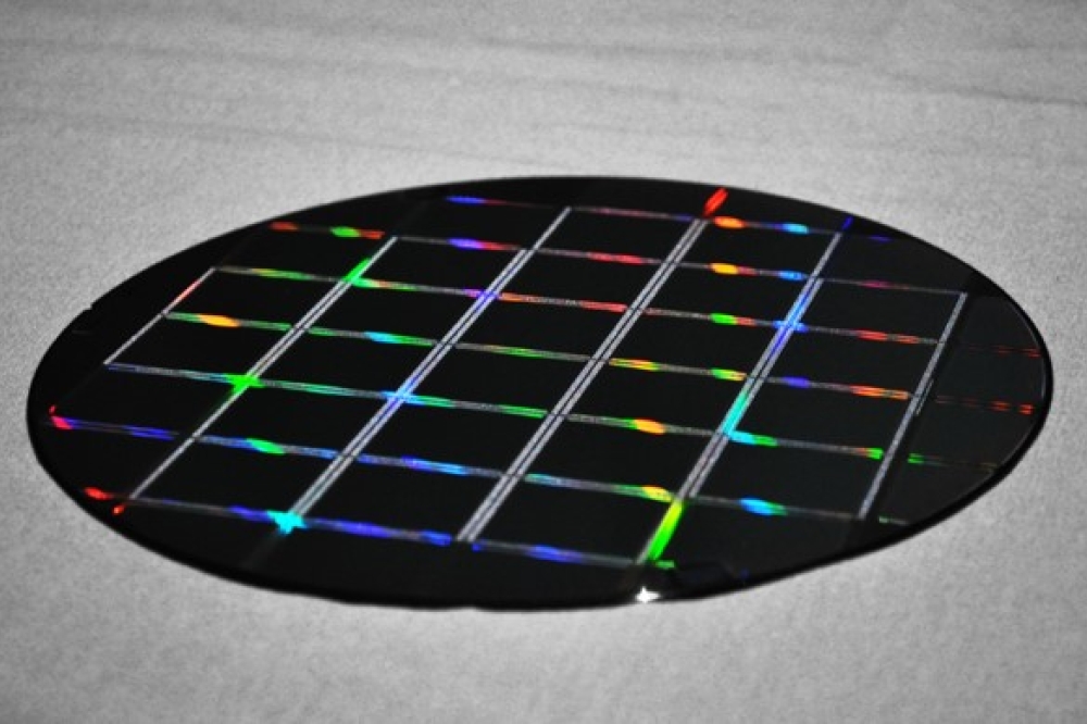
Metrology and inspection are essential for the management of semiconductor production, as they ensure the consistency and quality of the components being manufactured. Metrology refers to the measurement of various characteristics, such as dimensions and volume, using specialized equipment. On the other hand, inspection is the process of identifying defects or particles on semiconductor wafers, which are critical to ensuring the yield and quality of semiconductor products.
The growth of the semiconductor metrology and inspection market is driven by several factors. Advancements in research and development (R&D) facilities and the expansion of foundries have contributed significantly to market growth. Moreover, the increasing demand for consumer electronics has further fueled the need for accurate and efficient semiconductor production. The growing number of servers and data centers also plays a role in market expansion. As electronic devices continue to evolve, with demands for high performance, compact size, and cost-efficiency, the semiconductor industry has experienced a surge in demand for advanced inspection and metrology solutions, particularly in the 3D sector.
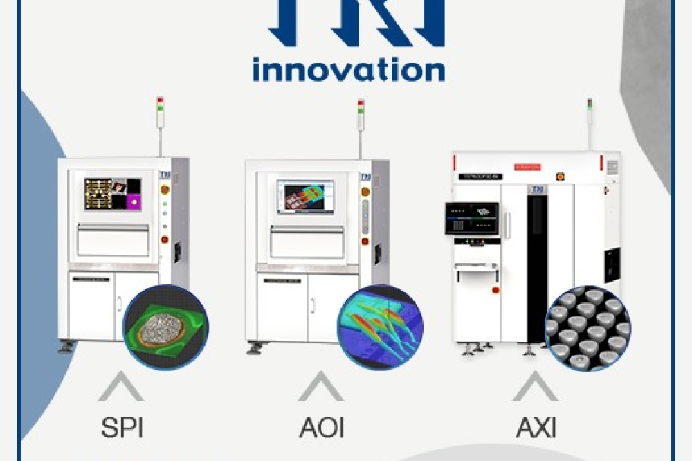
Key players in the market are adopting strategic initiatives such as mergers, acquisitions, collaborations, and product launches to strengthen their positions. For instance, in November 2021, Hitachi High-Tech introduced the GS1000 electron beam area inspection system. This newly developed tool offers fast and precise scanning electron microscope (SEM) inspections, further advancing the capabilities of the semiconductor metrology and inspection industry. Such innovations are expected to drive the market’s growth throughout the forecast period.
Regionally, Asia-Pacific held the largest share of the semiconductor metrology and inspection market in 2021. The region’s dominance can be attributed to the high concentration of integrated circuit (IC) manufacturers, which are major consumers of semiconductor metrology and inspection systems. Integrated circuits are used extensively in industries such as consumer electronics, telecommunications, data centers, automotive, and industrial sectors. Additionally, China has emerged as a leading player in the semiconductor production industry, accounting for approximately 45% of global production. China’s production capacity is expected to continue rising, with the nation projected to increase its share of global semiconductor production capacity from 15% to 24% over the next decade, according to the Financial Times.
Despite these positive trends, the COVID-19 pandemic posed significant challenges to the semiconductor metrology and inspection market. Factory shutdowns in key markets such as China, the U.S., and India disrupted the production and supply of semiconductor components. The pandemic also resulted in shortages of raw materials and a lack of workforce availability, leading to delays in manufacturing. However, the reopening of production facilities and the global rollout of vaccines have started to reverse these effects. As production resumes, the market is expected to recover, with continued growth driven by technological advancements and increasing demand.
The report also identifies several key findings that highlight the market’s dynamics. The wafer inspection system segment held the largest share in terms of revenue in 2021 and is expected to maintain significant growth throughout the forecast period. By technology, the optical segment generated the highest revenue in 2021 and is anticipated to continue its dominance in the coming years. Furthermore, the Asia-Pacific region is expected to witness the highest growth rate due to its thriving semiconductor manufacturing ecosystem.
In conclusion, the semiconductor metrology and inspection market is poised for significant growth, driven by advancements in technology, increased demand for consumer electronics, and the expansion of data centers and other high-tech industries. With ongoing developments and the reopening of global markets, the industry is expected to continue evolving and meeting the increasing demands of the semiconductor sector.


