Chiplets: revolutionising semiconductor design and manufacturing
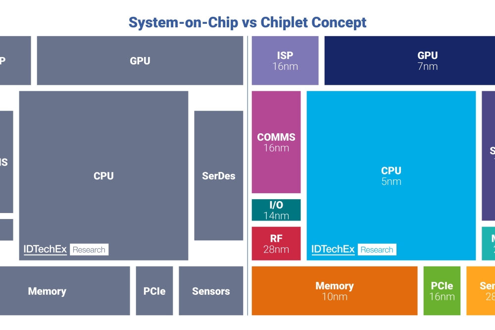
In the rapidly evolving world of semiconductors, chiplet technology is emerging as a groundbreaking approach that addresses many of the challenges faced by traditional monolithic System-on-Chip (SoC) designs, says Dr Xiaoxi He, Research Director at IDTechEx.
As Moore's Law slows down, the semiconductor industry is seeking innovative solutions to increase performance and functionality without merely increasing transistor density, as detailed in the IDTechEx report, "Chiplet Technology 2025-2035: Technology, Opportunities, Applications". Chiplets offer a promising path forward, providing flexibility, modularity, customizability, efficiency, and cost-effectiveness in chip design and manufacturing. Companies like AMD and Intel have been at the forefront of this technology, with products like AMD's EPYC processors and Intel's Ponte Vecchio data center GPU showcasing the potential of chiplets in boosting core counts and integrating diverse functionalities.
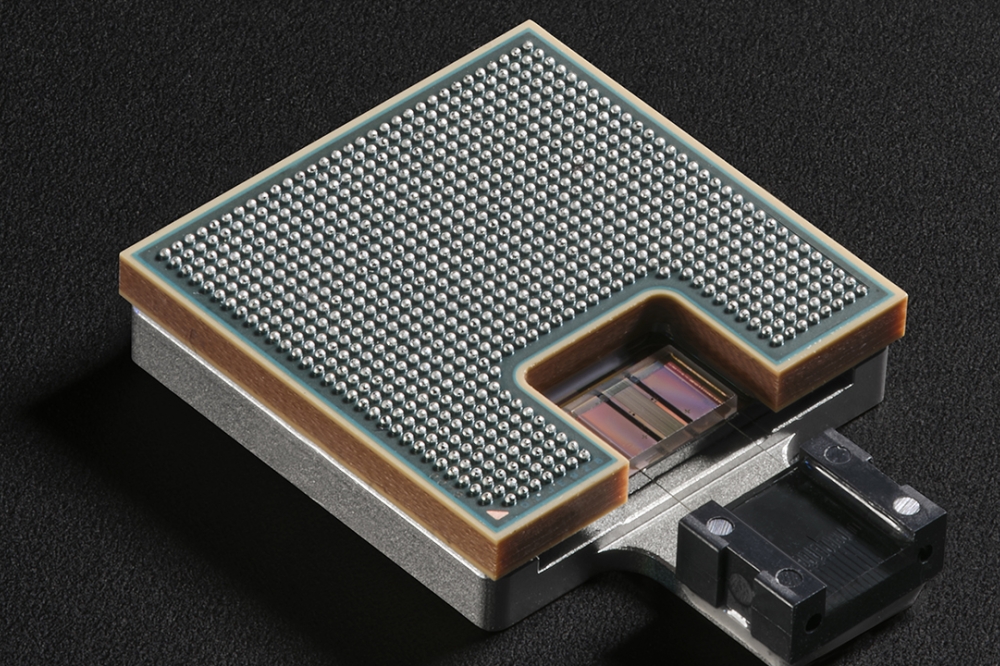
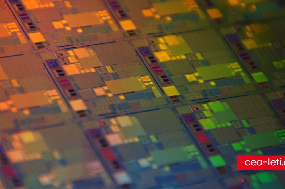
Chiplets are discrete modular semiconductor components co-designed and manufactured separately before being integrated into a larger system. This approach resembles an SoC on a module, where each chiplet is designed to function in conjunction with others, necessitating co-optimization in design. The modularity of chiplets aligns with key semiconductor trends such as IP chipletization, integration heterogeneity, and I/O incrementalization. Chiplet is also associated with heterogeneous integration and advanced packaging.
Why chiplets are gaining traction
The slowdown of Moore's Law has made it increasingly difficult to add more transistors within a limited area. Instead, the focus has shifted to enhancing function density - an area where chiplet design excels. In the meantime, development efforts have increasingly focused on system-level integration rather than solely on wafer manufacturing.
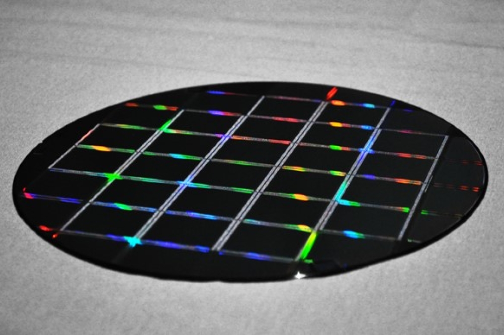
The adoption of chiplet technology is driven by its ability to address several critical limitations inherent in traditional monolithic chip designs. One advantage is its capacity to overcome constraints such as reticle size and the memory wall, which traditionally hinder the performance and scalability of semiconductor devices. By modularizing chip functions into discrete chiplets, manufacturers can optimize the use of semiconductor materials and processing nodes more effectively. In addition, chiplets can better utilize wafer corner space and have a lower defect rate on chips, which are often underutilized in conventional chip designs, particularly in larger SoCs that demand an increasing number of functions. The discrete components can be tested and validated individually before integration. As a result, the manufacturing yield increases, allowing for higher output quality and reduced costs per unit. Furthermore, chiplets facilitate a more flexible design process, enabling the integration of diverse functionalities tailored to specific applications without the need for entirely new chip designs. This flexibility reduces development time and costs and allows for rapid adaptation to evolving technological demands.
The nature of chiplets allows manufacturers to source different parts from multiple suppliers across various regions. This diversification reduces dependency on any single supplier or geographic area, thereby enhancing supply chain resilience. In the context of geopolitical tensions and trade restrictions, chiplet technology provides a strategic advantage by mitigating risks associated with supply disruptions. By adopting chiplet designs, companies can navigate these constraints more effectively, ensuring a steady supply of critical components without relying heavily on regions subject to political instability or trade sanctions.
Collectively, these factors make chiplet technology an attractive option for manufacturers seeking to enhance performance while maintaining economic efficiency.
Current market landscape
The global market for chiplets is experiencing remarkable growth and is projected to reach US$411 billion by 2035, driven by high-performance computing demands across sectors such as data centers and AI. The modular nature of chiplets allows for rapid innovation and customization, catering to specific market needs while reducing development timelines and costs.
While chiplets offer numerous advantages, they also present new challenges. The integration of multiple chiplets requires advanced interconnection technologies and standards to ensure seamless communication between components. Thermal management is another critical area, as increased function density can lead to overheating if not properly managed. These challenges open up opportunities for various players in the supply chain. For instance, different areas of the package in chiplet design require distinct types of underfill materials to address specific needs, e.g., to protect the chips themselves, providing mechanical support and thermal stability, as well as to safeguard the delicate wires and solder balls that connect the chiplets, preventing issues such as delamination or separation. This creates demand for innovative materials that enhance reliability and performance.
Report coverage
The IDTechEx report, "Chiplet Technology 2025-2035: Technology, Opportunities, Applications", provides a comprehensive analysis of the chiplet technology landscape, beginning with an executive summary that offers an overview of the report's findings and insights, setting the stage for a detailed introduction to the basics of chiplet technology. The report explores the drivers and benefits that make chiplet design attractive while identifying the challenges and hurdles in its adoption and implementation. It provides insights into technology and manufacturing processes, including design methodologies and packaging techniques. The discussion extends to inter-chiplet communication, focusing on interconnects and standards necessary for seamless integration. Thermal management strategies are outlined to address heat management in densely packed systems. Finally, the report examines various application areas, showcasing use cases across different sectors and demonstrating the versatility and impact of chiplet technology. A 10-year market forecast segmented by application that examines growth trends and future projections is provided. It also delves into the supply chain, highlighting key players and their roles in advancing chiplet technology.


