Tokyo Electron and IBM renew collaboration

New five-year agreement will focus on semiconductor and chiplet innovation for the age of generative AI.
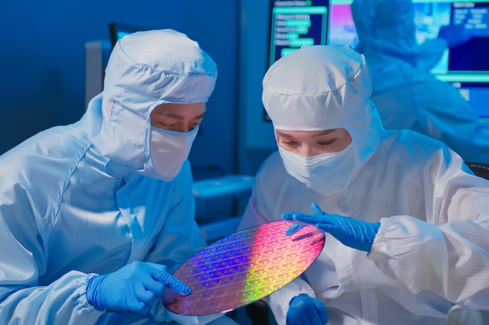
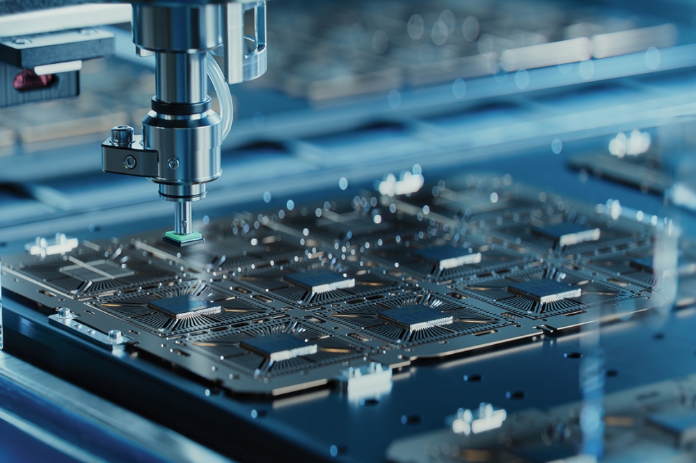
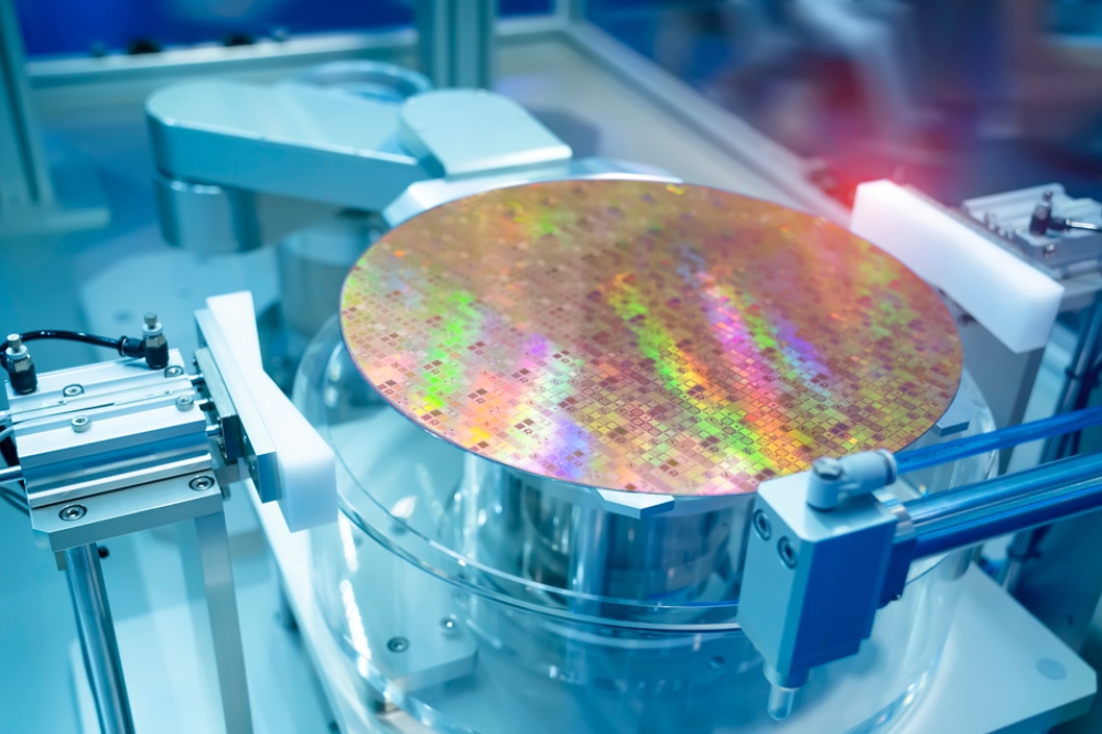
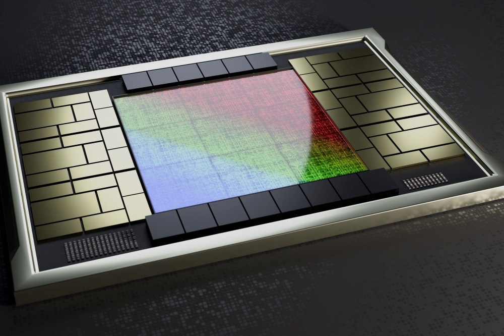
IBM and Tokyo Electron (TEL) have announced an extension of their agreement for the joint research and development of advanced semiconductor technologies. The new 5-year agreement will focus on the continued advancement of technology for next-generation semiconductor nodes and architectures to power the age of generative AI.
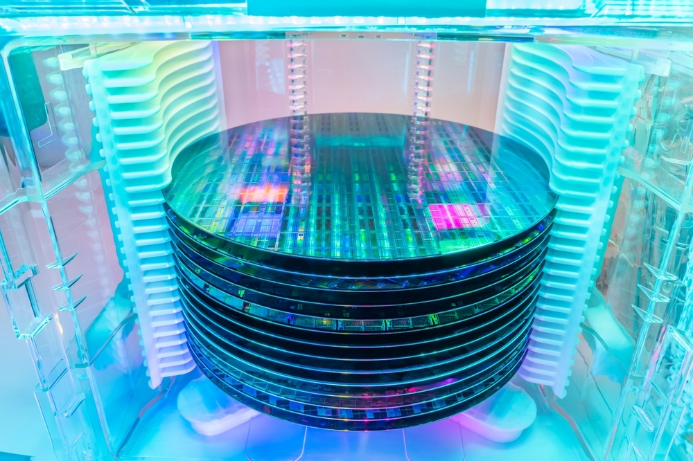
This agreement builds on a more than two-decade partnership between IBM and TEL for joint research and development. Previously, the two companies have achieved several breakthroughs, including the development of a new laser debonding process for producing 300 mm silicon chip wafers for 3D chip stacking technology.
Now, bringing together IBM's expertise in semiconductor process integration and TEL's leading-edge equipment, they will explore technology for smaller nodes and chiplet architectures to achieve the performance and energy efficiency requirements for the future of generative AI.
"The work IBM and TEL have done together over the last 20 years has helped to push the semiconductor technology innovation to provide many generations of chip performance and energy efficiency to the semiconductor industry," said Mukesh Khare, GM of IBM Semiconductors and VP of Hybrid Cloud, IBM. "We are thrilled to be continuing our work together at this critical time to accelerate chip innovations that can fuel the era of generative AI."
"IBM and Tokyo Electron have built a strong relationship of trust and innovation through years of joint development. We are excited to continue to build on our long-standing partnership with IBM for another five years. This renewed agreement underscores our mutual commitment to advancing semiconductor technologies, including patterning processes with High NA EUV." said Toshiki Kawai, Representative Director, President & CEO Tokyo Electron Limited. "Our collaboration at the Albany NanoTech Complex has been instrumental in driving innovation and we look forward to continuing this journey together."
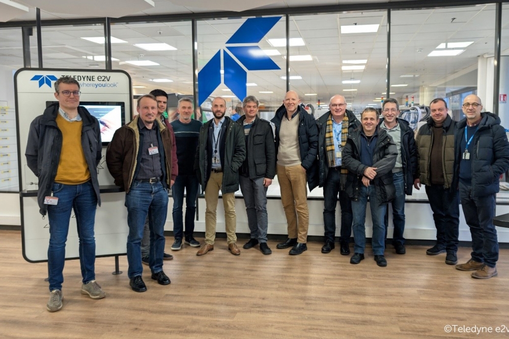
IBM and TEL are members of the Albany NanoTech Complex, the world's leading ecosystem for semiconductor research, owned and operated by NY CREATES. For years, IBM, TEL, and others have worked together to build the most advanced public-private semiconductor research facility to accelerate chip innovation. As a result, last year, the site was selected as America's first National Semiconductor Technology Center, the NSTC EUV Accelerator. As part of this new agreement, IBM and TEL researchers will continue to work together in Albany utilizing its unique ecosystem and R&D capabilities.