Intel shares technology roadmap

At the recent Intel Foundry Direct Connect, the company sharedprogress on multiple generations of its core process and advanced packaging technologies. The company also announced new ecosystem programs and partnerships, and welcomed industry leaders to discuss how a systems foundry approach enables collaboration with partners and unlocks innovation for customers.
Intel CEO Lip-Bu Tan opened the event by discussing Intel Foundry’s progress and priorities as the company drives the next phase of its foundry strategy. Naga Chandrasekaran, Intel Foundry chief technology and operations officer, and Kevin O’Buckley, general manager of Foundry Services, also delivered keynotes during the morning session, sharing process and advanced packaging news while highlighting Intel Foundry’s globally diverse manufacturing and supply chain.
Tan was joined on stage by ecosystem partners including Synopsys, Cadence, Siemens EDA and PDF Solutions to highlight collaboration in serving foundry customers. O’Buckley was joined by executives from MediaTek, Microsoft and Qualcomm.
“Intel is committed to building a world-class foundry that serves the growing need for leading-edge process technology, advanced packaging and manufacturing,” said Tan. “Our No. 1 job is to listen to our customers and earn their trust by creating solutions to enable their success. The work we are doing to drive an engineering-first culture across Intel while strengthening our partnerships throughout the foundry ecosystem will help us to advance our strategy, improve our execution and win in the market long term.”
The event announcements encompass core process and advanced packaging technology, a milestone in domestic U.S. manufacturing, and ecosystem support required to earn the trust of foundry customers. They include:
Process Technology
• Intel Foundry has engaged with lead customers on the Intel 14A process technology, the successor to Intel 18A. The company has distributed to lead customers an early version of the Intel 14A Process Design Kit (PDK), and multiple customers have expressed their intent to build test chips on the new process node.
• Intel 14A will feature PowerDirect direct contact power delivery, building on the PowerVia backside power delivery technology in Intel 18A.
• Intel 18A is now in risk production and expected to reach volume manufacturing this year. Intel Foundry’s ecosystem partners have electronic design automation (EDA) enablement, reference flows and intellectual property (IP) ready for production designs today.
• The new Intel 18A variant, called Intel 18A-P, is designed to deliver enhanced performance to a broader set of foundry customers. Early wafers based on Intel 18A-P are in the fab now. Because Intel 18A-P will be design rule-compatible with Intel 18A, IP and EDA partners have already started updating their offerings for the variant.
• Intel 18A-PT is another new variant that builds on Intel 18A-P performance and power efficiency advancements. Intel 18A-PT can be connected to top die using Foveros Direct 3D with hybrid bonding interconnect pitch less than 5 micrometers (µm).
• Intel Foundry’s first production 16 nanometer (nm) tape-out is in the fab now, and the company is engaging with lead customers on a 12nm node and derivatives built in collaboration with UMC.
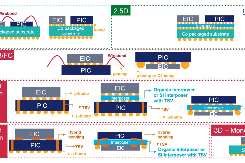
Advanced Packaging
• Intel Foundry offers system-level integration using Intel 14A on Intel 18A-PT, connected via Foveros Direct (3D stacking) and embedded multi-die interconnect bridging (2.5D bridging).
• New advanced packaging technology offerings include EMIB-T to enable future high bandwidth memory needs and two new additions to the Foveros architecture: Foveros-R and Foveros-B provide additional efficient and flexible options for customers.
• A new engagement with Amkor Technology increases customer flexibility in choosing the right advanced packaging technology for their needs.
Manufacturing
• Fab 52 in Arizona has successfully “run the lot,” marking the first wafer processed through the facility, demonstrating progress in domestic manufacturing of leading-edge Intel 18A wafers. Intel 18A volume production will begin in Intel’s Oregon fabs as Arizona manufacturing ramps later this year. Intel 18A and Intel 14A research, development and wafer production will all be U.S.-based.
Ecosystem
• New programs have been added within Intel Foundry’s Accelerator Alliance – Intel Foundry Chiplet Alliance and Value Chain Alliance – along with a range of announcements from top ecosystem partners.
Delivering Trusted Ecosystem Tools and IP
Intel Foundry is supported by a comprehensive portfolio of IP, EDA and design services solutions delivered by trusted, proven ecosystem partners to drive advancements beyond traditional node scaling. As the newest program in Intel Foundry’s Accelerator Alliance, the new Intel Foundry Chiplet Alliance will initially focus on defining and driving infrastructure on advanced technology for government applications and key commercial markets. The Intel Foundry Chiplet Alliance will provide an assured and scalable path for customers looking to deploy designs that leverage interoperable and secure chiplet solutions for targeted applications and markets. (Quote Sheet: Introducing the Intel Foundry Chiplet Alliance)
The Intel Foundry Accelerator Alliance also includes IP Alliance, EDA Alliance, Design Services Alliance, Cloud Alliance and USMAG Alliance.