Building the fabric of quantum networking
While quantum processors continue to advance, a critical challenge remains: how to scale from today's few-hundred qubit systems to the millions needed for practical applications?
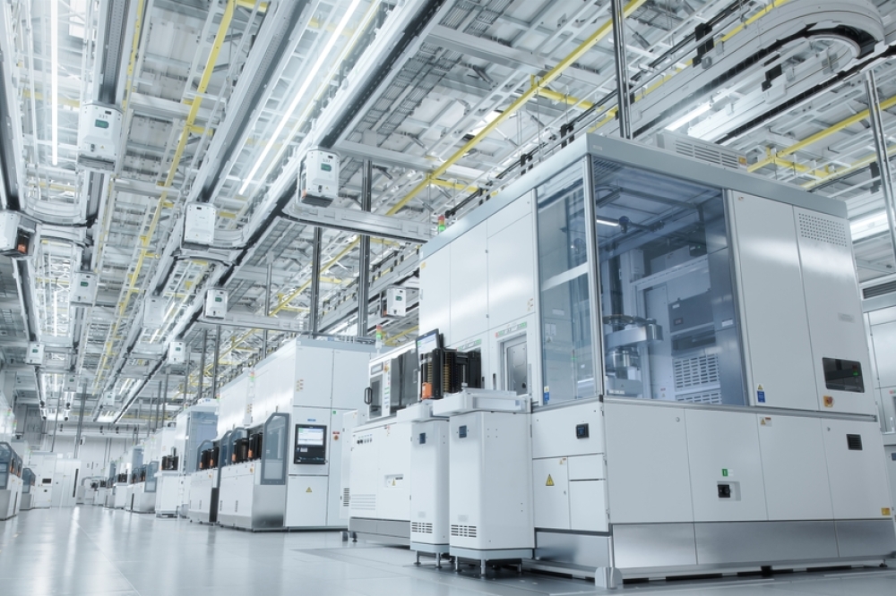
Cisco Quantum Labs says that it is building the quantum networking infrastructure that will make distributed quantum computing a reality years sooner than previously thought possible. This infrastructure will simultaneously enable innovative use cases in the classical world today.
Reimagining data centres for the quantum era
Cisco’s arXiv paper "Quantum Data Center Infrastructures," introduces an architecture for quantum data centers. The challenges for quantum data center network fabric are fundamentally different from classical ones.
Quantum data centers must preserve fragile quantum states, distribute entanglement resources, facilitate teleportation between processors and synchronize operations with sub-nanosecond precision. These capabilities are not in commercial off-the-shelf networking components.
The quantum data center architecture Cisco has developed consists of three layers:
1. A physical layer of specialized quantum hardware;
2. An entanglement management layer that distributes quantum resources; and
3. A computing layer that partitions algorithms across networked processors
This architecture enables multiple smaller quantum processors to work together as a unified system, potentially accelerating practical quantum applications by years.
Engineering the entanglement source
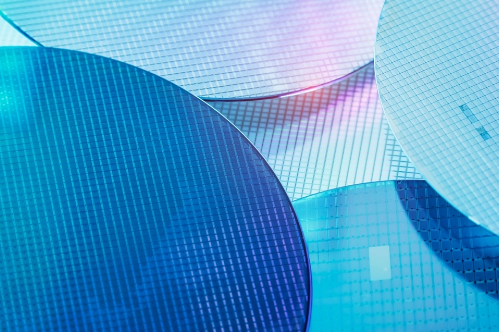
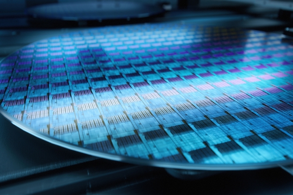
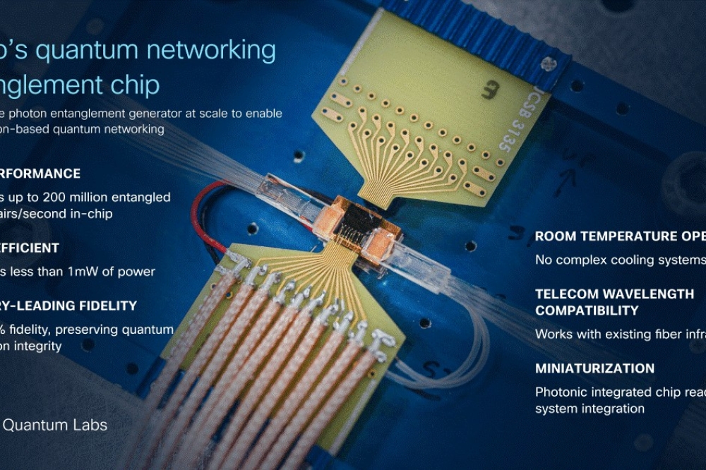
One of the fundamental components in Cisco’s architecture is its quantum network entanglement chip— a quantum networking device that creates pairs of photons that remain connected regardless of distance.
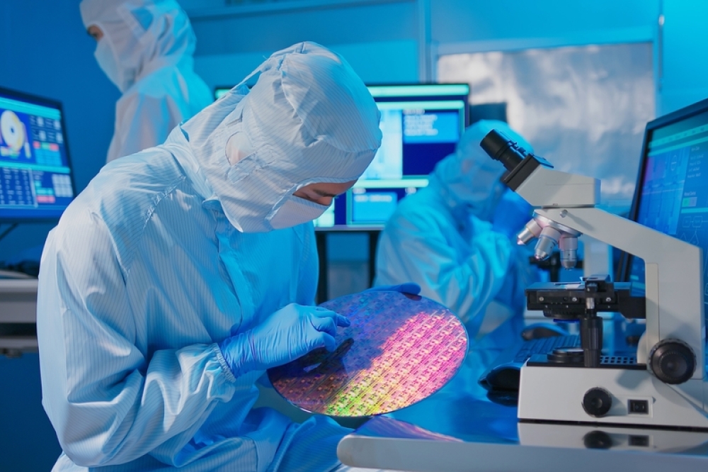
Developed in collaboration with UC Santa Barbara, the prototype:
• Leverages spontaneous four-wave mixing in III-V semiconductor waveguides on a silicon wafer platform;
• Generates over one million useable entangled photon pairs per second per channel (up to 200 million pairs per second in the chip);
• Achieves as high as 99% fidelity while consuming less than 1 mW of power, at room temperature;
• Enables the creation of arrays of entanglement sources on the same chip for massive multiplexing for high rate end-to-end and multi-user quantum networking making it the brightest chip scale source today; and
• Operates at 1550 nm telecom wavelengths, integrating with existing fiber infrastructure - a critical advantage for real-world deployment.
This breakthrough was in part made possible through academic collaboration with UC Santa Barbara.
Professor Galan Moody, who worked with Cisco, explains: “We’re excited to collaborate with Cisco to co-develop entanglement sources for their quantum network. Integrated photonics enables many sources to be combined onto a single chip, and by packaging these sources with optical fiber and electronic controls, a single device can boost the entanglement rates for many users on their quantum network.”
Cisco’s research extends beyond this initial entanglement source. In collaboration with a startup organization, the company is also experimenting with a complementary technology using rubidium vapor cells that bridges different quantum systems that operate in different frequencies in our data center architecture.
This dual-frequency source creates entangled pairs where one photon operates at near-IR frequency (close to most quantum computing platforms) while its partner operates at telecom frequency, solving a key integration challenge for heterogeneous quantum environments.
Beyond entanglement: A complete quantum network
A quantum network requires fundamentally new components that work at the quantum mechanics level. When building a quantum network, it’s not possible to digitize information as in classical networks - quantum properties must be preserved throughout the entire transmission path. This requires specialized hardware, software, and protocols unlike anything in classical networking.
Cisco research encompasses the entire quantum networking stack:
• Quantum switches: Traditional optical switches would destroy quantum information. Cisco’s switch design uses waveguides that can route quantum information without measurement or observation, preserving the delicate quantum states. This switch design is insensitive to environmental noise and operates with high precision timing to maintain quantum coherence.
• Quantum Network Interface Cards (NICs): Similar to classical NICS, these components connect quantum processors to the network while managing the challenging conversion between computing frequencies and networking frequencies. Different quantum computing technologies can connect through Cisco’s vendor-agnostic approach.
• Distributed computing compiler: This multi-tenant software partitions quantum algorithms across processors and schedules entanglement distribution. It can map and translate complex quantum circuits to physical hardware while preserving quantum advantages across the distributed system.
From prototype to production
Cisco is working with design partners across quantum computing, telecommunications, and financial services to refine our technologies. Financial institutions are particularly interested in secure communication, decision coordination, and ultra-precise time synchronization for various trading applications—applications that can leverage quantum networking today, even before full-scale quantum computers are available.
The future of quantum computing doesn't lie in massive monolithic systems but in networked quantum data centers. This mirrors the evolution of classical computing, which reached its full potential only after networked systems emerged.
Rather than seeing quantum networking as a distant future technology, Cisco views it as the critical path for accelerating the quantum timeline. By intelligently networking smaller quantum processors, Cisco can achieve the scale needed for practical applications years ahead of expectations.
(This news is based on a Cisco blog authored by Ramana Kompella and Reza Nejabati).