3D-Micromac introduces next-generation Laser Sample Preparation Platform
microPREP® L delivers 'unmatched' sample size scalability, high throughput and precision, and automation-ready workflows for advanced semiconductor failure analysis.
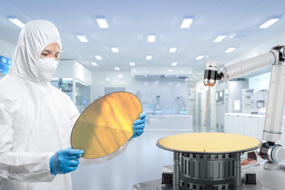
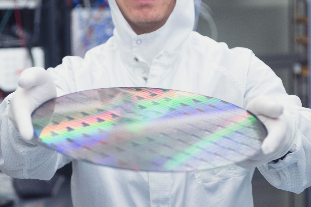
3D-Micromac AG has introduced microPREP® L—the latest addition to its microPREP family of laser-based sample preparation systems, which is designed to support sample sizes up to whole 12-inch (300-mm) wafers and system-level boards. This new platform enables fast, precise, reproducible, and non-destructive material removal at scale, delivering significant productivity gains for failure analysis, process development, and quality assurance in the semiconductor and electronics industries. Multiple samples can be prepared at different locations on the wafers or system-level boards within a single workflow, without process restarts.
The new microPREP L system will be featured at the upcoming International Symposium for Testing and Failure Analysis (ISTFA), taking place Nov. 16-20 in Pasadena, Calif. Attendees are invited to visit 3D-Micromac at Booth 318 to learn more and speak with company representatives about this breakthrough technology.
Overcoming Sample Preparation Bottlenecks
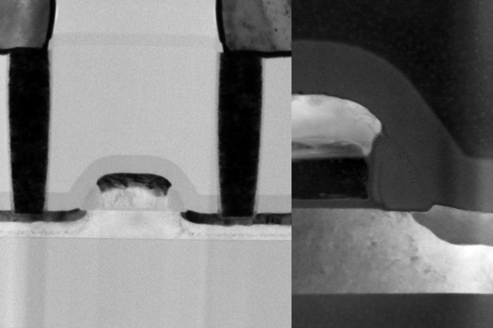
Sample preparation remains one of the most time-consuming and costly steps in semiconductor failure analysis. Traditional preparation methods like mechanical polishing and focused ion beam (FIB) milling cannot meet the stringent needs of today’s advanced applications. Mechanical polishing introduces mechanical stress to the specimen, which can affect the overall quality and yield. FIB milling is constrained by limited ablation rates, very small sample sizes, high tool operating costs, and the need for highly trained operators, making it impractical for large-scale or production-adjacent use.
Integrated sample prep systems that combine laser and FIB tools in a single platform introduce capacity bottlenecks, as only one function can operate at a time. These systems also suffer from particle contamination, which can compromise the integrity of the sample and downstream analysis.
microPREP L: A Dedicated, Scalable Alternative
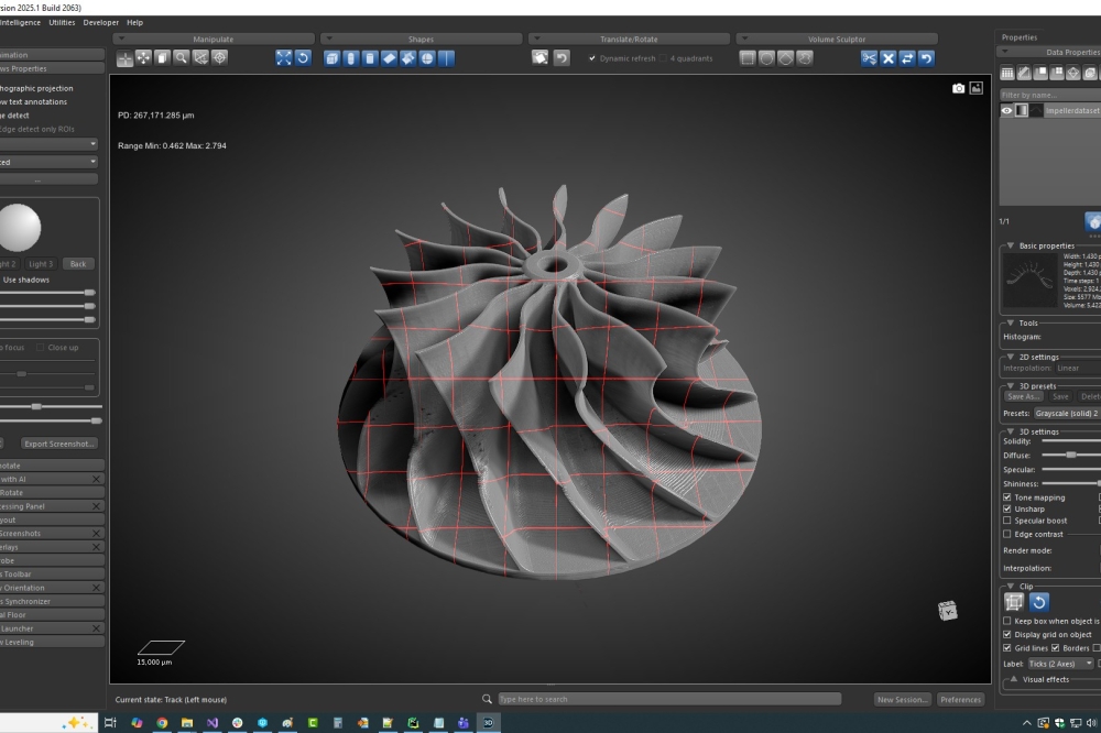
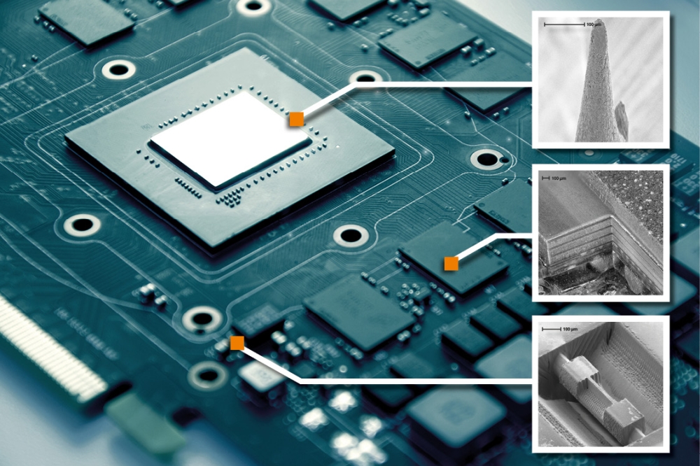
Unlike hybrid platforms, the new microPREP L system is a dedicated, standalone laser micromachining solution that delivers precision, speed, and sample size scalability without compromise. Leveraging selective laser ablation and newly integrated real-time process monitoring, the system enables micrometer-level targeting and nondestructive removal of material—even from large and complex assemblies such as advanced semiconductor packages, printed circuit boards, and whole 12-inch wafers.
By supporting system-level preparation without cutting up the sample into smaller pieces, this platform helps preserve device integrity, accelerating failure localization and analysis. These capabilities also enable failure analysis to be extended beyond the lab and into fab environments, where rapid root-cause analysis is critical to improving yield and uptime.
Key Features and Benefits
· Sample Scalability: Supports whole wafers up to 12 inches and large board-level devices—enabling failure analysis in both lab and fab environments—while offering a roadmap for even larger samples in future system extensions
· Selective Laser Ablation: Enables precise, localized material removal without destroying or damaging the regions of interest
· In-Situ Process Monitoring: Real-time depth sensing and ablation control ensures high accuracy—reducing rework and improving overall yield in failure analysis workflows
· Automated Workflows: Designed for high-throughput and repeatable operation with minimal operator intervention
· Multi-Sample Workflow Efficiency: Since the microPREP L can handle much larger sample sizes, customers can prepare multiple samples directly on the wafers or system-level boards in a single workflow without process restarts
· FIB/SEM Workflow Integration: Offloads bulk removal to the laser system, optimizing downstream tool use
· Customizable Recipes: Flexible for diverse materials and geometries
Significant Productivity Gains
In benchmark tests, a single operator using the microPREP L was able to prepare up to 32 samples per day, sufficient to feed up to seven plasma FIB systems—dramatically increasing throughput and reducing overall time-to-sample. In another case, a task that took just 23 minutes on the system would have taken up to six months using traditional gallium FIB milling.
“As semiconductor devices become more complex with the rise of heterogeneous integration, multi-layer architectures, and tighter development cycles, traditional sample preparation methods are no longer sufficient for advanced process development and failure analysis,” stated Uwe Wagner, CEO of 3D-Micromac AG. “Our new microPREP L system addresses these challenges head-on by enabling fast, precise, and damage-free sample prep at the wafer and system level. With its unmatched scalability and automated workflows, microPREP L is designed to meet the evolving needs of advanced semiconductor sample prep in both R&D and production environments.”