Maximising advanced packaging hinges on manufacturing process optimisation
Unlocking packaging’s promise will require solving upstream manufacturing process bottlenecks and rethinking global semiconductor supply chain strategies.
By Dr. Maksym Plakhotnyuk, CEO and Founder, ATLANT 3D
AI chip revenue is soaring, driven by breakthrough models and unprecedented demand across the GPU and ASIC segments.
This rapid growth benefits semiconductor manufacturers, as each new AI generation requires ever-larger quantities of leading-edge silicon to deliver improved cost, performance, and efficiency per operation.
To keep pace with this demand – and transcend the physical limits of classic transistor scaling—advanced packaging technologies, especially 3D stacking and chiplet architectures, have become a vital frontier. These techniques integrate multiple chips and components (such as CPUs,
GPUs, memory, and high-speed interconnects) in a single heterogeneous package.
By minimizing the physical distance between elements, advanced packaging improves data transmission rates and energy efficiency, a key factor in the escalating technological rivalry between the U.S. and China.
Leading foundries and outsourced semiconductor assembly and test (OSAT) players are responding. Notably, TSMC has announced a $100 billion U.S. investment plan – including a next-generation advanced packaging facility in Arizona – while Intel recently expanded its advanced packaging operations in New Mexico, aiming for domestic supply chain resilience.
Such moves are further catalyzed by policy incentives and tariff structures designed to onshore semiconductor manufacturing capacity.
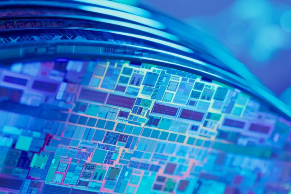
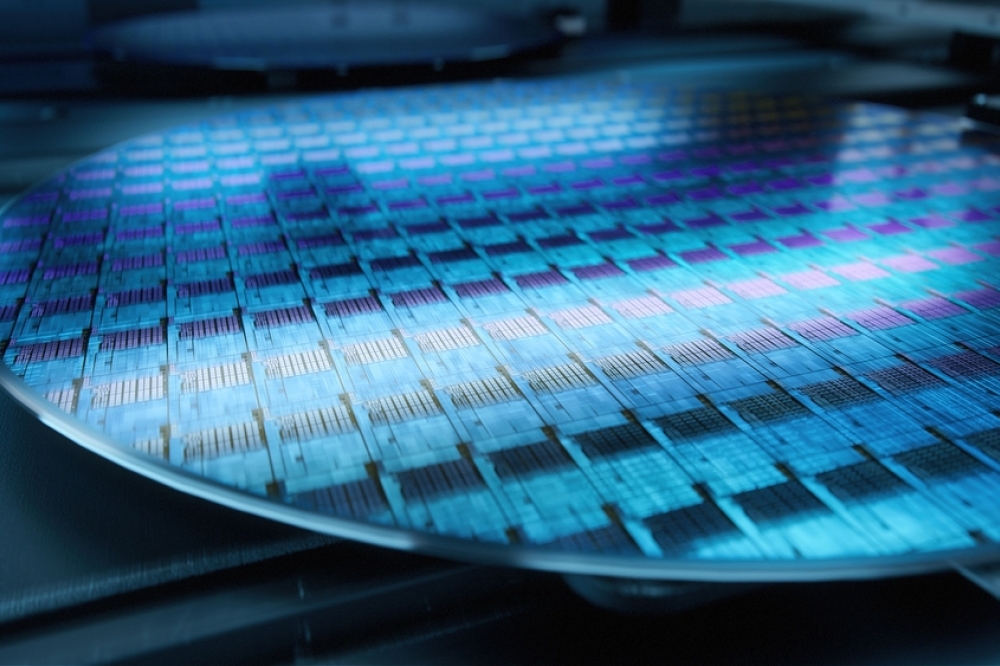
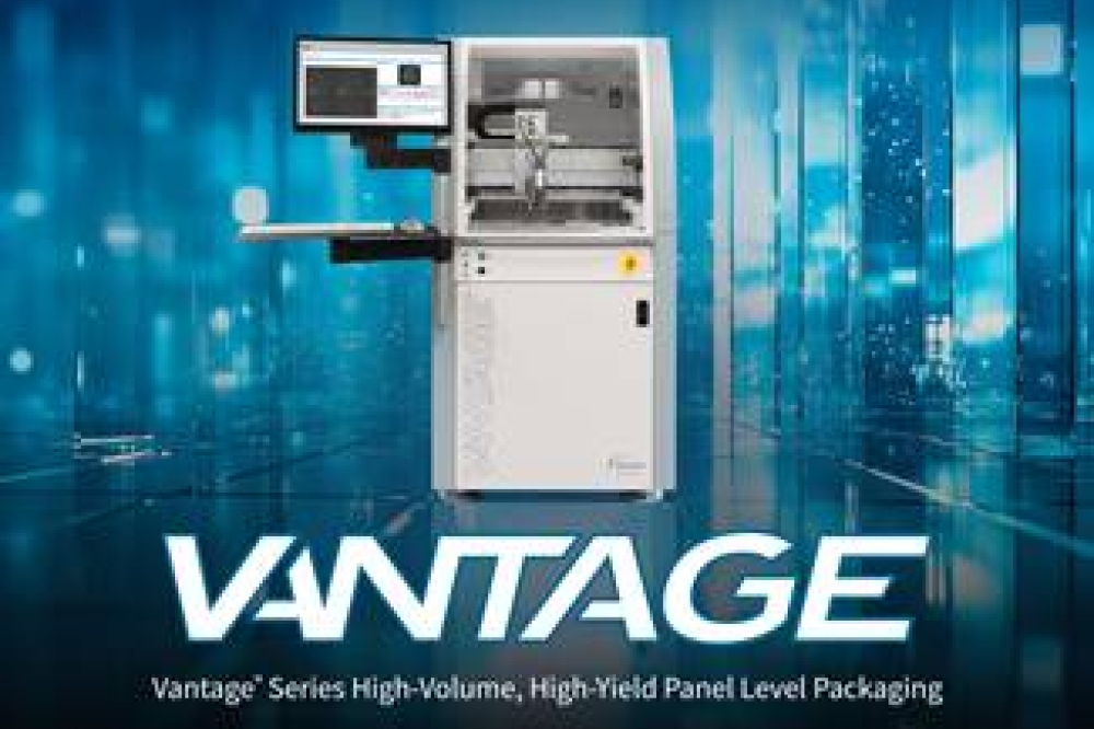
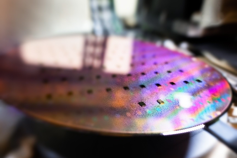
Despite these advances, challenges remain. Advanced packaging is highly complex, involving tightly integrated stacks of diverse materials and structures – such as interposers, redistribution layers (RDLs), and multiple active and passive chips.
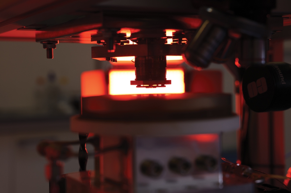
Conventional thin-film approaches like atomic layer deposition (ALD) offer atomic-scale precision but generally lack the throughput or process simplicity required for large-scale packaging. Direct-write additive manufacturing techniques like DALP are emerging to address some of these bottlenecks, enabling more flexible and rapid construction of advanced packages with lower material waste, fewer processing steps and the same precision as ALD.
Meanwhile, the infrastructure that houses AI chips must evolve. Next-generation AI accelerators and advanced packages require new datacenter designs – with upgraded power delivery, cutting-edge cooling, and higher rack densities – to avoid bottlenecks that would offset performance and sustainability gains from packaging improvements.
While advanced packaging reduces the energy needed for interconnects, the aggregate power draw for hyperscale AI datacenters continues to rise in line with massive computational demand.
Crucially, high-volume advanced packaging capacity in the U.S. is not expected to be available before mid-2027, and U.S.-designed chips like NVIDIA’s Blackwell family continue to be routed to Taiwan for packaging.
This gap creates opportunities for other countries to accelerate local industry development, and exposes U.S. manufacturers to additional costs and potential tariffs if products must be re-imported after overseas packaging – potentially eroding domestic cost advantages.

Industry consensus is forming around the idea that advanced packaging may be as critical as transistor innovation itself for the future of AI and semiconductors. As NVIDIA CEO Jensen Huang noted,
“To meet [AI’s] demand, advanced packaging has become as critical as transistor design in delivering the efficiency and power our customers require.” But fully unlocking packaging’s promise will require solving upstream manufacturing process bottlenecks and rethinking global semiconductor supply chain strategies.
Advanced packaging holds the potential to shift power balances not just within AI, but also in fields such as defense, biomedical engineering, and energy, provided nations and firms can adapt their supply chains, infrastructure, and manufacturing processes for a new era of integrated, high-performance computing.
 DR. MAKSYM PLAKHOTNYUK, CEO AND FOUNDER, ATLANT 3D