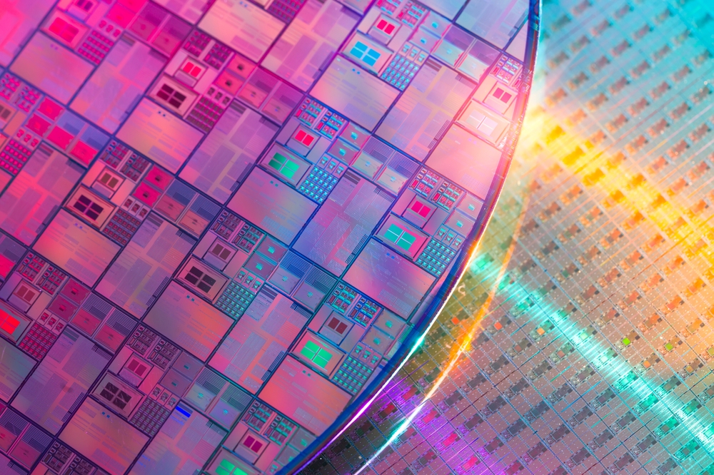
Inspiring innovations address key industry challenges

Imec has been busy in recent weeks, unveiling a tool for AI data centre design and optimization and presenting research results, including mitigating thermal bottleneck in 3D HBM-on-GPU architectures using a system-technology co-optimization approach, demonstrating the first wafer-scale fabrication of solid-state nanopores using EUV lithography, advancing 2D-material based device technology beyond state of the art and successfully integrating colloidal quantum dot photodiodes (QDPDs) on metasurfaces developed on 300mm CMOS wafers.
At the recent Super Computing 2025 event, the premier international conference and exhibition for high performance computing (HPC), imec launched imec.kelis, a cutting-edge analytical performance modeling tool designed to revolutionize the design and optimization of AI datacenters. Early adopters are already experimenting with the tool, signaling strong market interest.
The AI datacenter landscape is undergoing rapid transformation. As workloads scale to trillions of parameters and energy demands surge, system architects face mounting pressure to balance performance with sustainability and cost. Traditional simulation methods are often slow, opaque, or too narrow in scope. Imec.kelis addresses this gap by offering a fast, transparent, and validated modeling framework that enables informed decision-making across the full stack—from chip to datacenter.
It empowers teams to explore architectural trade-offs, optimize resource allocation, make informed decisions, and accelerate innovation in a field where time-to-insight is critical. Imec.kelis provides an end-to-end framework for evaluating system performance across compute, communication, and memory subsystems. It is tailored for large language model (LLM) training and inference workloads, offering fast, accurate, and generalizable predictions validated on industry-standard platforms such as Nvidia A100 and H100. The tool builds on imec’s proven track record in analytical performance modeling for high-performance computing (HPC) and artificial intelligence (AI). It leverages imec’s system-level modeling and performance analysis for compute, communication, and memory subsystems, especially in the context of large-scale AI datacenters and large language model (LLM) workloads, imec’s hardware-software- codesign expertise, and semiconductor technology roadmap.
“Imec.kelis is more than a simulator – it’s a strategic enabler for the next generation of AI infrastructure,” said Axel Nackaerts, imec’s System Scaling lead. “By combining hardware-software- codesign, we empower system architects to make informed decisions at datacenter scale.”
Key Features:
- LLM task-graph analyzer and parallelism mapper
- Hierarchical roofline model and topology-aware communication library
- Interactive dashboard for real-time design space exploration
- Validated within 12% error margin for large-scale LL
“In a test case, we used imec.kelis to compare the performance (defined as training time for GPT3), for different GPU architectures and scaling nodes, at plotted performance against cost, showcasing the flexibility of the tool for various purposes, such as architecture exploration, future technology projection, and co-optimization. Our results show that imec.kelis enables careful validation of performance and helps identify key insights for architecture exploration and future technology projection.” stated Nackaerts.
Imec.kelis v1.0 will be available for licensing starting Q1 2026. The tool has already attracted early adopters, signaling strong market interest.
NanoIC adds advanced SRAM memory macros to its N2 pathfinding PDK
Meanwhile, at SEMICON Europe, the NanoIC pilot line, a European initiative coordinated by imec and dedicated to accelerating innovation in chip technologies beyond 2nm, announced the release of the N2 P-PDK v1.0, an important update of its N2 Pathfinding Process Design Kit (P-PDK). This new version introduces several new features, including a library of 29 SRAM memory macros, allowing designers to explore and benchmark system-on-chip (SoC) designs with frontside and backside power routing. By adding the SRAM macros in the design options, the N2 P-PDK v1.0 marks an important milestone in enabling research, learning, and design exploration on advanced and future nodes.

imec.kelis
Towards next-generation SoC designs
As chip technologies scale beyond 2nm, the ability to explore full System-on-Chip (SoC) architectures with novel technology enablers becomes increasingly important. SoCs, integrating logic, memory, and interconnect capabilities into a single chip, are the backbone of a wide variety of digital applications, from smartphones and AI accelerators to automotive controllers. However, early-stage SoC design exploration is often constrained by limited access to complete and realistic design kits that include advanced or future technology scaling boosters such as power delivery networks. This gap makes it difficult for designers to validate architectural concepts, experiment with emerging technologies, or to train the next generation of chip designers on advanced nodes.
NanoIC’s low-barrier N2 P-PDK v1.0 aims to bridge this gap, offering instant access to a wide variety of new design features, including a portfolio of 29 ready-to-use SRAM macros with both frontside and backside power routing configurations.
This dual configuration, offered for the first time in a pathfinding PDK, enables designers to experiment with and optimize memory integration within realistic, advanced power networks.
As a result, NanoIC’s N2 P-PDK v1.0 now provides the building blocks of a complete SoC as well as the architectural context to explore how those blocks interact within realistic power networks. It enables users to move beyond simple logic design and explore and validate full SoC systems that reflect the challenges and opportunities of next-generation semiconductor design.

Lowering barriers for learning and exploration
By making these advanced features freely available to academic researchers, startups, and design teams, NanoIC significantly lowers the barriers to innovation, empowering the development of next-generation applications, and strengthening Europe’s position in the global semiconductor landscape.
“This v1.0 version of our N2 P-PDK enables designers to evaluate the impact of new technology features and integration options on their designs before they exist in foundry offerings. It provides a unique environment to connect technology pathfinding with practical design enablement, ensuring that breakthroughs in device research translate into system-level advances.”, Marie Garcia Bardon, Department Director at imec and work package leader within the NanoIC pilot line, summarizes.
Building on the learnings from the previous N2 P-PDK, this release lays the groundwork for future PDK iterations, launching additional advanced logic, memory, and interconnect PDKs in the coming years. The roadmap includes future versions of the N2 P-PDK, as well as upcoming A14 and A7 logic P-PDKs, eDRAM and SOT memory PDKs, and advanced interconnect solutions (RDL, hybrid bonding, interposers), empowering innovation across the full spectrum of next-generation chip technologies.
To support designers in exploring the full capabilities of the N2 P-PDK v1.0, a dedicated workshop will be organized on March 25-26, 2026. This session will offer a theoretical framework, followed by hands-on training sessions, using two different EDA tools: Cadence and Synopsys. Participants will gain insights into the SRAM memory macros, updated design rules, and system-level integration strategies. More details and registration will be made available via the NanoIC website.
Mitigating thermal bottleneck in 3D HBM-on-GPU architectures
At the 2025 IEEE International Electron Devices Meeting (IEDM), imec presented that is believed to be the first thermal system-technology co-optimization (STCO) study of 3D HBM-on-GPU (high-bandwidth memory on graphical processing unit), a promising compute architecture for next-gen AI applications. By combining technology and system-level mitigation strategies, peak GPU temperatures could be reduced from 140.7°C to 70.8°C under realistic AI training workloads – on par with current 2.5D integration options. The result demonstrates the strength of combining cross-layer optimization (i.e., co-optimizing the knobs at all the different abstraction layers) with broad technological expertise, a combination that is unique to imec.
Integrating high bandwidth memory (HBM) stacks directly on top of graphical processing units (GPUs) offers an attractive approach for building next-gen compute architectures for data-intensive AI workloads. This 3D HBM-on-GPU promises a huge leap forward in compute density (with four GPUs per package), memory per GPU, and GPU-memory bandwidth compared to current 2.5D integration options where HBM stacks are placed around (one or two) GPUs on a silicon interposer. However, the aggressive 3D integration approach is prone to thermal issues because of higher local power density and vertical thermal resistance.
At 2025 IEDM, imec presented the first comprehensive thermal simulation study of 3D HBM-on-GPU integration that not only identifies thermal bottlenecks but also proposes strategies to increase the architecture’s thermal feasibility. Imec researchers show how co-optimizing technology and system-level thermal mitigation approaches can reduce peak GPU temperatures from 141.7°C to 70.8°C under realistic AI training workloads.
The model assumes four HBM stacks –
each consisting of twelve hybrid-bonded DRAM dies – placed directly on top of a GPU using microbumps. Cooling is provided on top of the HBMs. Power maps derived from industry relevant power profiles are applied to identify local hotspots and compare them to a 2.5D baseline. Without thermal mitigation strategies, the 3D model yields a peak GPU temperature of 141.7°C – far too high for GPU and HBM operation – while the 2.5D integration benchmark peaks at a workable 69.1°C under the same cooling conditions. We used these data as a starting point to evaluate the joint impact of technology and system-level thermal mitigation strategies. Technology-level strategies include, among others, HBM stack merging and thermal silicon optimization. On the system-level side, we assessed the impact of double-sided cooling as well as GPU frequency scaling.
James Myers, System Technology Program Director at imec: “Halving the GPU core frequency brought the peak temperature from 120°C to below 100°C, achieving a key target for the memory operation. Although this step comes with a 28% workload penalty (i.e., a slowdown of AI training steps), the overall package outperforms the 2.5D baseline thanks to a higher throughput density offered by the 3D configuration. We are currently using this approach to study other GPU/HBM configurations (e.g., placing GPUs on top of HBMs), anticipating future thermal constraints.”
Julien Ryckaert, Vice President Logic Technologies at imec: “This is also the first time that we demonstrate the capabilities of imec’s cross-technology co-optimization (XTCO) program in building more thermally robust compute systems. XTCO was launched in 2025 to efficiently align imec’s technology roadmaps with key industry system scaling challenges and is built on four critical system level pillars: compute density, power delivery, thermal, and memory density and bandwidth. It combines our STCO/DTCO mindsets with imec’s broad technology expertise – a unique combination that is of great value in addressing the growth and diversification of compute system demands. We invite companies from within the entire semiconductor ecosystem, including fabless and system companies, to join our XTCO program and collaboratively resolve critical system scaling bottlenecks.”
The first wafer-scale fabrication of solid-state nanopores using EUV lithography

At IEDM 2025, imec also presented the first successful wafer-scale fabrication of solid-state nanopores using extreme ultraviolet (EUV) lithography. Solid-state nanopores are emerging as powerful tools for molecular sensing but haven’t been commercialized yet. This proof of concept is a crucial step towards their cost-effective (mass) production.
Solid-state nanopores are tiny holes - just a few nanometers wide - etched into Silicon Nitride membranes. When immersed in fluid and connected to electrodes, they allow individual molecules to pass through, generating electrical signals that can be analyzed in real time. Because the pore size can be easily adjusted, they offer a wide range of applications, from virus identification to DNA and protein analysis. This label-free, single-molecule detection method is key to next-generation diagnostics, proteomics, genomics, and even molecular data storage applications.
Biological nanopores, on the other hand, formed by proteins in lipid membranes, have enabled commercial sequencing platforms, but they are limited by stability and integration challenges. Solid-state nanopores overcome these limitations with robustness, tunability, and compatibility with semiconductor manufacturing, making them ideal for scalable, high-throughput sensing. But achieving nanometer-level precision and uniformity in solid-state pores across large areas remains a challenge.
Current fabrication techniques are often slow and limited to the lab, delaying their widespread use for sensing applications.
In a new paper presented at IEDM 2025, imec reports successful fabrication of highly uniform nanopores with diameters down to ~10nm across full 300mm wafers.
The team combined EUV lithography with a spacer-based etch technique to achieve nanometer-level precision and reproducibility - two long-standing challenges in nanopore technology.
The nanopores were embedded in silicon nitride membranes and electrically characterized in aqueous environments. Translocation experiments with DNA fragments also confirmed high signal-to-noise ratios and excellent wetting behavior, validating the nanopores’ sensing performance with biological material.
“Imec is uniquely positioned to make this leap. We can apply EUV lithography - traditionally reserved for memory and logic - to life sciences. By leveraging our lithography infrastructure, we’ve shown that solid-state nanopores can be fabricated at scale with the precision needed for molecular sensing,” said Ashesh Ray Chaudhuri, first author and R&D project manager at imec. “This opens the door to high-throughput biosensor arrays for healthcare and beyond.”
Looking ahead, this feat can enable rapid diagnostics, personalized medicine, and molecular fingerprinting. Building upon the EUV nanopore advancements, imec is currently developing a modular readout system with scalable fluidics as a platform for application relevant chemistry development. The team invites life science tool developers to use this platform to test their concepts and requirements.
At the 2026 IEEE International Solid-State Circuits Conference (ISSCC), the paper “A 256-Channel Event-Driven Readout for Solid-State Nanopore Single-Molecule Sensing with 193 pArms Noise in a 1 MHz Bandwidth” was presented, showcasing a proof-of-concept ASIC readout developed by imec, to support next-generation custom nanopores.
Advancing 2D-material based device technology beyond state of the art
Again at the IEDM, imec also presented breakthrough performance of p-type FETs with monolayer WSe2 channels, and improved fab-compatible modules for source/drain contact formation and gate stack integration. These results, achieved through collaborations with leading semiconductor manufacturers, mark a significant advance for 2D-material based technology, which is considered a promising long-term option for extending the logic technology roadmap.
Replacing Si conduction channels with atomically thin layers made of 2D transition metal dichalcogenides (MX2) promises to enable ultimate gate and channel length scaling, while maintaining good electrostatic channel control and high carrier mobility. Crucial milestones to be achieved include high-quality 2D-material layer deposition, gate stack integration, low-resistance source/drain contact formation, and 300mm fab integration. Also, while most efforts focus on improving n-type devices (with channels made of WS2 or MoS2), more fundamental work is needed on p-type devices, which require different channel materials (such as WSe2).
Gouri Sankar Kar, VP R&D compute and memory device technologies at imec: “At 2025 IEDM, we show in two separate presentations how in-depth collaborations with leading semiconductor manufacturers within imec’s core CMOS Industrial Affiliation Program (IIAP) have enabled breakthroughs in the performance of 2D-material based devices. In both partnerships, combining high-quality 2D material layers provided by the manufacturer with imec’s optimized contact and gate modules played a key role in pushing the technology beyond state of the art.”

Figure 1: Cross section and transfer curves of WSe2 devices.
“Depositing the top-gate HfO2 dielectric on top of a MX2 channel requires an additional seed layer to support HfO2 nucleation and growth”, explains Gouri Sankar Kar. “For nFETs, this is solved by creating an AlOx interfacial layer, but this approach is challenging for pFETs due to the different characteristics of the WSe2 channel material as compared to its n-type counterparts. In partnership with TSMC, we started with a synthetic bilayer of WSe2, which was formed by subsequently transferring two high-quality WSe2 monolayers from TSMC on our substrates. We then oxidized the top WSe₂ monolayer, converting it into an interfacial layer that successfully supported the deposition of the HfO₂ gate oxide. This fab-compatible lab-based integration approach resulted in record performance of our dual-gated pFETs.”

Figure 2: Selective etch process resulting in AlOx interlayer lateral removal
Another presentation highlights the collaboration between imec and Intel in developing 300mm manufacturable modules for source/drain contacts and gate stack integration, for n-type (WS2 and MoS2) and p-type (WSe2) 2D-FETs. “The key innovation consists in applying a selective oxide etch process on Intel’s high-quality 2D material layers, that were capped with an interfacial AlOx layer, a HfO2 layer and a SiO2 layer”, Gouri Sankar Kar explains. “The oxide etch process allowed the formation of fab-compatible damascene-style top contacts – a world first. In addition, during the vertical contact etch process, the interfacial AlOx layer was simultaneously etched laterally, removing AlOx from the channel region. This significantly lowered the top gate’s EOT benefitting the gate’s transfer characteristics.”
This research was funded by the imec IIAP Exploratory Logic program, the 2D-PL pilot line project through Horizon Europe (101189797) and Horizon 2020 (952792) grant agreements.
Overcoming the cost and complexity barriers of traditional SWIR sensors
Finally at IEDM 2025, imec successfully demonstrated the integration of colloidal quantum dot photodiodes (QDPDs) on metasurfaces developed on its 300 mm CMOS pilot line. This pioneering approach enables a scalable platform for the development of compact, miniaturized shortwave infrared (SWIR) spectral sensors, setting a new standard for cost-effective and high-resolution spectral imaging solutions.
Unlocking new possibilities in SWIR sensing
Short-wave infrared (SWIR) sensors offer unique capabilities. By detecting wavelengths beyond the visible spectrum, they can reveal contrasts and features invisible to the human eye and can therefore see through certain materials such as plastics or fabrics, or challenging conditions like haze and smoke. Conventional SWIR sensors remain, however, expensive, bulky, and challenging to manufacture, restricting their use to niche applications. Quantum dot (QD) image sensors, a new class of SWIR sensors, offer a promising alternative, combining lower cost with higher resolution. So far, however, they have operated in broadband rather than in spectral mode.
Imec addresses this challenge by successfully cointegrating colloidal quantum dot photodiodes (QDPDs) with metasurfaces developed on its 300 mm CMOS pilot line. Quantum dots are nanoscale semiconductors that can be tuned to absorb specific infrared wavelengths, while metasurfaces are nano-patterned ultra-thin layers that precisely control how light interacts with the sensor. By combining these elements in a CMOS-compatible process, imec has created a scalable platform for miniaturized SWIR spectral detectors, delivering a compact, high-resolution sensor architecture that can be manufactured using standard CMOS processes.
“What particularly sets this technology apart is its scalability,” says Vladimir Pejovic, R&D project lead at imec. “Traditional quantum dot image sensors require redesigning complex photodiode layers for every wavelength, which makes adjustments to each application’s spectrum complex and costly. Our approach shifts that complexity to the CMOS level, using metasurfaces to tune spectral response instead of altering the photodiode stack. This opens the door to easily customizable high-resolution spectral SWIR sensors and paves the way for new features in areas such as security, agriculture, automotive, aerospace, and beyond.”
Accelerating innovation through collaboration
This breakthrough is the result of a multidisciplinary effort, uniting imec’s expertise in quantum dot image sensors, flat optics (metasurfaces), and spectral imaging. The next step is to scale this technology from proof of concept to low volume, and ultimately, full-scale manufacturing. To accelerate this transition, imec invites partners to collaborate.
“Our ambition is to turn this breakthrough into an industry-ready platform,” Pawel Malinowski, imec portfolio manager, explains. “We want to work with partners to develop custom image sensors and integrated devices, demonstrating this technology in real-world applications. By combining imec’s spectral expertise, quantum dot know-how, and advanced CMOS process capabilities with specific application domains, we aim to accelerate innovation and bring next-generation SWIR sensors from proof-of-concept to full-scale manufacturing. Imec therefore welcomes collaboration with partners to help shape the future of sensing and imaging together.”