Silicon photonics needs a new packaging strategy to reach volume
The schedule for silicon photonics has accelerated due to
demands from AI and large data centers.
By Sylvain Dulphy, Finetech
The joint display by Nvidia and Mercedes at CES 2026 of a commercial autonomous vehicle signaled that high-volume applications of photonic components exist today. Yet, a major obstacle remains before the industry achieves the mass manufacturing scale required by the 2030 roadmap. The primary constraint has shifted: it is no longer front-end lithography only, but the packaging process itself. Reaching the 2030 targets depends on a fundamental shift in how the industry views the “backend” process.

The value shift to fifty percent
Semiconductor packaging was traditionally viewed as a
commodity, a final step handled in lower-cost regions. In standard products,
this stage represents roughly 15 percent of the total value. In advanced
photonics for data centres and AI, that ratio has flipped. Packaging now holds
up to 50 percent of the final product value.
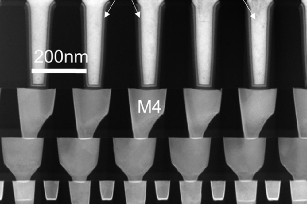
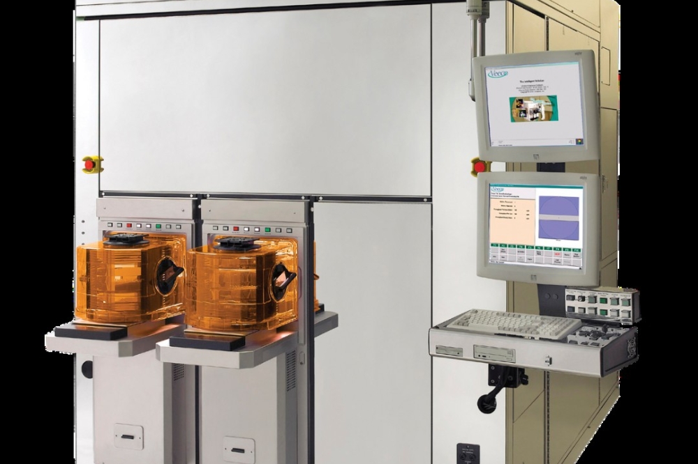
Advanced processes such as copper-to-copper hybrid bonding, championed by leaders like TSMC, are erasing the traditional division between standard packaging side by side assembly and wafer fabrication. These steps are migrating from standard assembly lines into high-end cleanrooms to address new steps like die to wafer bonding, chiplets, usage of interposer. At these scales, the precision required is absolute.
“If the packaging is compromised, the entire product is lost,” notes Sylvain Dulphy, Sales
Manager at Finetech. “Regardless of the quality of the 2-nanometer chip inside, if the packaging is not executed perfectly, the unit is discarded.” Packaging has turned from a protective shell into a functional performance requirement.
Moving beyond pluggables
To support the signal speeds AI workloads demand, the sector is transitioning from external pluggable
optics to co-packaged solutions. The objective is to drastically reduce the
distance the signal travels within the chip, “external” signals being optical.
“If the electrical signal path is too long, it effectively becomes a filter,” explains Dulphy. “It is similar to the concept of power in physics, which requires both force and velocity. You might have speed, but if the connection length diminishes your signal strength, your global performance is capped.”
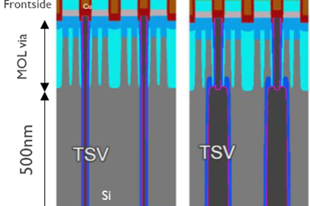
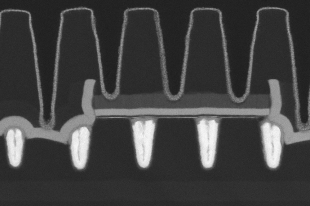
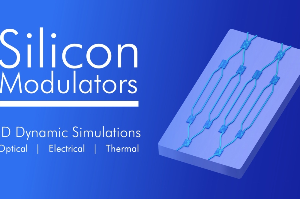
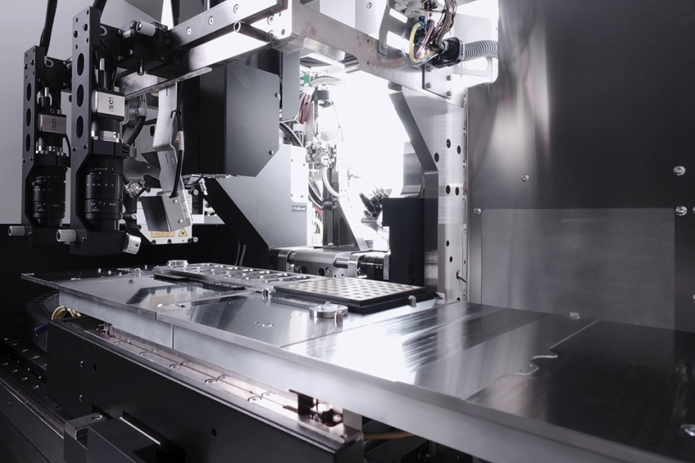
To maintain both signal integrity and speed, connections must be immediate. This necessitates the use of bumps or metal-to-metal contacts via interposers and chiplets. While this integration allows for the miniaturization needed for high-volume products—from LiDAR in cars to medical tools—it introduces a new manufacturing hurdle linked to alignment in 3D of all those elements.
With today’s technologies in semiconductor foundry, this is achievable, but now we mix optical and electrical in the same chip with mixed materials. We therefore need to make assemblies of chip that are not thermally homogeneous so not compatible with same process profiles and we need to optically align them.
Solving optical alignment
For silicon photonics to reach volumes similar to mobile
phone parts, the industry must fix the optical alignment issue. Today, aligning
a fiber to a light source often uses active alignment of single elements. This
involves a slow loop of moving, turning on the laser, reading the signal, and
adjusting again.
This cycle lacks the speed required for semiconductor volumes. It costs too much and takes too long. Research now points to passive alignment methods. The goal is to use intermediate parts designed to guide light beams without requiring powered checks for every unit. Mastering passive methods is the only way to reach the cost structures needed for mass adoption.

The supply chain gap
As we look to 2030, the supply chain readiness poses a
greater obstacle than the technology itself. The sector currently lacks
standards, so each player invents their own way, which limits broad growth.
Furthermore, the equipment supply is under pressure. Developing a new class of machine from the ground up takes years. We cannot wish for the tools to exist; they must develop alongside the technology. This is causing a convergence where traditional front-end semiconductor tool makers are now looking at packaging steps. Partnering with an existing packaging specialist is probably the most effective combination.
The message is plain. Hardware limits software. The limits we solve today define what future AI code can do. But to solve them by 2030, tool makers, foundries, and institutes must set their schedules now. The volume is coming; the question is if the supply chain can handle it.