How materials will unlock the future of advanced packaging
As transistor scaling reaches its physical limits, advanced
packaging has become the critical enabler of next-generation semiconductor
performance, powering the shift from 2D scaling to 3D integration, chiplets,
and trillion-transistor systems.
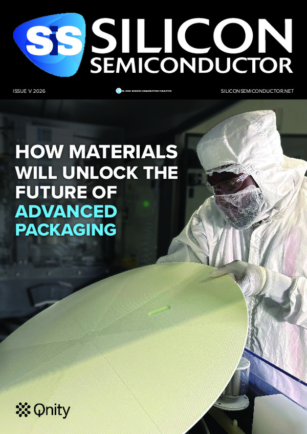
By Jon Kemp, CEO, Qnity
For decades, the story of our industry was a single word: shrink. Moore’s Law made transistors smaller, and their size didn’t compromise speed and power. This isn’t the case anymore. We’ve reached the physical limits of what shrinking alone can deliver, and a new era is taking its place — one I’d sum up in a different word: stack. The industry is moving from flat, 2D chip designs to vertical, 3D architectures, and that shift puts pressure on materials, integration, and reliability that the old playbook was never built to handle.
This move from “shrink” to “shrink and stack” is forcing the entire ecosystem to think differently. Advanced packaging is the strategic enabler that makes this shift possible — the link that lets manufacturers push transistor architecture and density while holding the line on performance, efficiency, and reliability. When architectures go vertical, you can’t bolt on the materials, interconnects, and packaging at the end. They have to be designed in from the very first step.
The customer base is widening, too. More companies across the ecosystem now have a direct stake in advanced packaging and 3D integration, and OEMs are increasingly in the room for investment, material selection, and design decisions. More complexity means more demand — for innovation, for specialized talent, and for advanced manufacturing capacity across the board.
We’ve seen significant transitions before. Most recently, it was the shift to gate-all-around (GAA) transistor architecture — a shift powered by a multi-year effort to develop and optimize the materials needed to meet the stringent demands of 2nm logic at high yields. When manufacturers debuted 2nm in 2025, it quickly became the most competitive process node among the world’s biggest tech companies, prized for the transistor density and energy efficiency that have become critical gains for AI.
But those advances remain within the bounds of traditional scaling. What we’re facing today is different: performance is no longer defined only at the transistor. It is increasingly defined at the package.
The future of chipmaking depends on how entire systems are integrated, and meeting the sophisticated advanced packaging requirements that every new “stack” demands. That’s where our role at Qnity becomes even more pivotal. Leveraging decades of expertise, we’re delivering the materials solutions to the transistor and advanced packaging challenges of the angstrom era.
The angstrom era
The next evolution in transistor architecture is the complementary field-effect transistor (CFET), a more advanced 3D design that will free up space, increase density, and deliver faster performance at lower power. Imec predicts its commercial introduction around 2033.
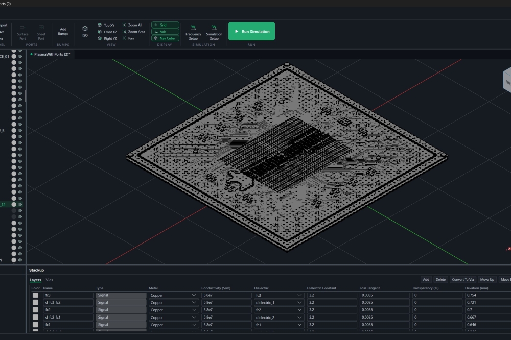
In parallel, the world’s largest logic chipmakers are already moving towards angstrom-class nodes. But the industry’s ultimate target of trillion-transistor systems on a chip package by 2030 cannot be achieved through scaling alone. Packaging is pushing boundaries today, but the dual demands of trillion-transistor density and more advanced architectures call for a fundamental leap — denser connections, more sophisticated signal routing, and packaging schemes capable of coordinating an exponentially complex web of chip-to-chip communication.
First, the industry has to reckon with physics. As transistors shrink and the power density of a chip increases, quantum effects like electron leakage and heat buildup grow more significant, and they put a hard ceiling on how far miniaturization can go.
Getting to the required density will lean on techniques like 3D stacking and chiplet integration — and those bring challenges of their own: managing power, heat and EMI, while wiring together a lot more chips in a lot less space.
That makes thermal management critical. A trillion transistors on a single chip system demands enormous energy and throws off unprecedented heat. Power delivery is already a major challenge. But thermal management may be the bigger test — because if you can’t remove heat efficiently, you don’t have a high-performing, reliable system. You have a limit.
Forming all of those interconnects presents the third constraint. As transistor counts climb, so does the complexity of linking logic and memory. Traditional methods of making copper-based interconnects are running into limits on speed, efficiency, and latency that require new techniques.
As our partners and customers have reckoned with these difficulties, each challenge points to the same answer: advanced packaging. Done right, it addresses design complexity, power management, communication bottlenecks, and system integration all at once.
Advanced packaging as the invisible infrastructure
As transistor counts rise, the complexity of integrating logic, memory, and specialized processors into one cohesive system grows exponentially. But there’s a deeper problem underneath the density problem, and it comes down to communication.
Here’s something that doesn’t get enough attention. Even as individual chips get faster, comparatively little industry-wide investment has gone into the technologies that let chips exchange data efficiently. In AI and high-performance computing, a significant share of data center energy goes to powering the connections between chips. Those connections generate heat through electrical resistance, require cooling, and create bottlenecks.

Consider this: in some advanced AI systems, a processor can sit idle roughly 30% of the time, simply waiting for data to arrive from memory. That idle time is fewer computations, higher costs, and performance left on the table — and at scale, the waste is staggering. The idle power burned during that 30% across a modern AI compute cluster runs on the order of 200 MWh a year — enough to fully charge 2,500 electric vehicles.
Advanced packaging attacks those inefficiencies head-on. Techniques like 3D stacking and chiplet integration raise density by combining multiple chips into a single package, and they improve communication, cut latency, and optimize power distribution. Heterogeneous integration goes further still — combining chips with specialized roles, like AI accelerators, memory modules, and high-speed controllers, into one highly tuned system. Each component gets optimized for its job, and that’s what powers the workloads defining this moment: real-time language model inference, autonomous vehicle perception, complex scientific simulation, and next-generation gaming engines.
Thermal management is becoming an even more critical part of the equation, too. Advanced packaging brings in thermal interface materials (TIMs) and interposers that dissipate heat efficiently and keep chips at their peak. Paired with high-density interconnects, chip-to-chip bonding, and emerging optical connections, these solutions keep data moving fast even across the most densely packed architectures.
Put it together, and advanced packaging resolves the core bottlenecks — communication, power, and thermal management — that stand between today’s chips and tomorrow’s potential. It’s the invisible infrastructure that modern semiconductors are built on.
Qnity’s approach to advanced packaging
Building on a legacy of more than 50 years, Qnity offers a full spectrum of technology solutions across the advanced packaging ecosystem — from wafer processing and interposer integration to IC substrates and panel-level packaging. By pairing deep expertise in semiconductor front-end and back-end processes with expertise in PCB manufacturing, we help manufacturers design fit-for-purpose systems that maximize compute efficiency, power management, and performance-per-cost.
Advanced packaging demands precision at every stage, and our materials and process technologies are built for exactly that. Planarization pads, slurries, and cleans reduce defects across complex architectures. Fine-feature photoresists enable the high-resolution patterning that next-generation IC substrates require. Metallization solutions support high-density interconnects — including through-silicon vias (TSVs) for stacked memory (HBM) and microbump interconnects — so chips communicate efficiently and reliably.
Materials are only part of it. Our process development infrastructure supports end-to-end evaluation and optimization. Test vehicle builds help identify failure modes and refine design rules, so stacked chips, interposers, and IC substrates perform reliably under real conditions. Panel-level packaging and interposer demo capabilities extend that control across wafer- and system-level integration, supporting both IC substrates and next-generation PCB fabrication.
By combining materials expertise, process knowledge, and system-level integration, Qnity’s innovations let technologies like 3D stacking, chiplet integration, and heterogeneous integration operate at scale. That’s how manufacturers get past the real pain points — chip-to-chip communication, interconnect efficiency, thermal management, and high-density scaling.

The future of advanced packaging
More advanced 3D architectures, larger substrates, multi-reticle fabrication, higher transistor densities — the angstrom era creates new pressure at every level.
Advanced packaging doesn’t just support scaling compute clusters and AI systems over the next five years. It lays the foundation for the even more forward-looking high-density, high-performance chips that come after.
To get ready for what’s next, we strategically differentiate our R&D investment to our top 10 innovation programs, spanning advanced-node fabrication, advanced packaging, IC substrate and PCB manufacturing, along with thermal management and EMI technologies. Our longer-term bets explore the emerging materials and technologies that could define the next round of breakthroughs. By enabling customer and industry roadmaps and anticipating long-term trends, we’re focused on solving the immediate technical challenges and helping shape the next generation of semiconductor systems at the same time.
Our technology solutions enable effective communication, manage thermal loads, and support heterogeneous integration — helping manufacturers realize the full performance potential of transistor systems in the trillions, while preparing for what lies beyond 2030.
The stack era begins
There’s no longer any real doubt: advanced packaging has gone from a supporting technology to a strategic enabler. It bridges the gap between what’s physically possible on a chip and what’s practically achievable in a complete system.
This is a turning point in how our industry approaches design, integration, and performance. We must challenge our assumptions across transistor miniaturization, interconnect efficiency, thermal management, and system-level integration.
At Qnity, our success is defined by an ecosystem-wide perspective. We bring materials expertise, process development, application engineering, and system-level integration together to take on the full spectrum of technical challenges — from wafer processing and interposers to IC substrates and panel-level packaging.
The next generation of high-performance semiconductor systems won’t succeed on transistor scaling alone. It will depend on sophisticated integration, advanced materials, and forward-looking process design.
If “shrink” built the last era, “stack” will help shape the next. And we’ll be there — helping the industry unlock the full potential of the chip designs that power the AI, high performance computing, and advanced connectivity breakthroughs of the coming decade and beyond.