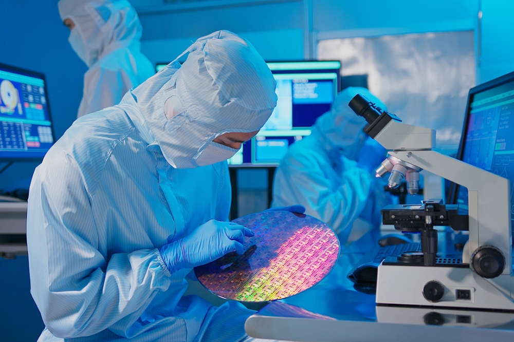
Unleashing the intelligence revolution
TSMC’s 2026 Europe Technology Symposium revealed how AI is
reshaping the semiconductor industry, driving advances in leading-edge logic,
advanced packaging, photonics and system-level integration while accelerating
the path to a trillion-dollar market.
Key takeaways from TSMC’s 2026 europe technology symposium
At its 2026 Europe Technology Symposium, TSMC delivered a
clear and emphatic message: the semiconductor industry has entered a new era
defined by artificial intelligence, and the pace of change is accelerating
faster than previously anticipated. What emerged from the event was not just an
update on process nodes or packaging technologies, but a comprehensive vision
of how silicon will underpin an “Intelligence Revolution” that extends from data centres
to autonomous systems and into the physical world.
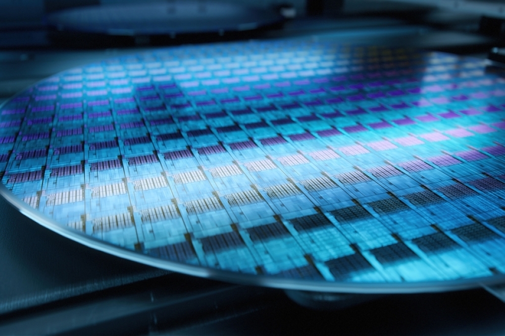
From advanced logic and 2nm-class innovations to 3D
integration, photonics, and system-level design, TSMC outlined a roadmap that
reflects both unprecedented demand and increasing architectural complexity. At
the same time, the company provided a broader market context, revealing how AI
is reshaping the economics, priorities and trajectory of the semiconductor
sector.
A trillion-dollar industry arrives
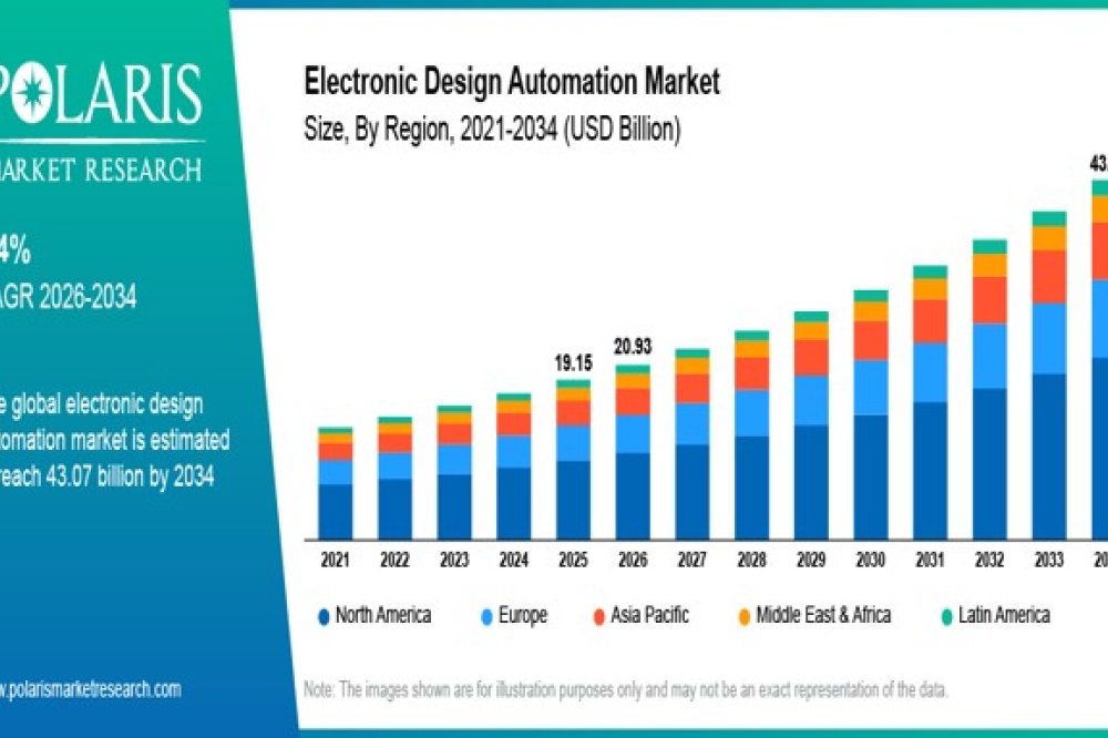
One of the most striking announcements from the symposium
was the revised outlook for the global semiconductor market. While earlier
projections suggested that the industry would reach the US$1 trillion milestone
by 2030, TSMC now expects that threshold to be exceeded as early as 2026.
Looking further ahead, the market is forecast to reach approximately US$1.5
trillion by the end of the decade.
This accelerated growth is overwhelmingly driven by high-performance computing and AI, which together are expected to account for roughly 55% of total semiconductor demand. Smartphones remain a significant segment at around 20%, while automotive and IoT applications each contribute approximately 10%. The remaining share is distributed across other emerging and legacy applications.
What is particularly important in this context is the evolving nature of AI workloads. The industry is transitioning from a phase dominated by model training to one increasingly defined by inference, where trained models are deployed at scale to generate outputs in real time. This shift is critical because inference workloads are far more widely distributed, spanning cloud data centres, edge devices and embedded systems.
The concept of “tokens”, whether words, images or data points generated by AI systems, is central to this transformation. As token generation increases, so too does the demand for compute resources. This creates a powerful feedback loop in which higher productivity drives further investment in AI infrastructure, which in turn increases demand for advanced silicon.
The implication is clear: semiconductor growth is no longer tied solely to traditional computing cycles. Instead, it is increasingly driven by the exponential scaling characteristics of AI itself.
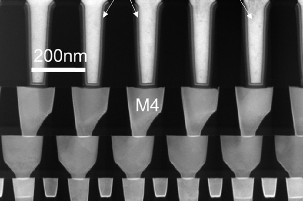
The evolution of transistor technology
At the core of TSMC’s roadmap is the continued evolution of
transistor architectures. The industry has already moved from planar
transistors to FinFETs and is now firmly transitioning to nanosheet (or
gate-all-around) structures. These developments have enabled continued scaling
in performance, power efficiency and density, even as physical limits become
more challenging.
Looking beyond nanosheet architectures, TSMC is exploring complementary field-effect transistor (CFET) designs, which involve vertically stacking n-type and p-type transistors. This approach represents a potential pathway for extending Moore’s Law by increasing transistor density without requiring further horizontal scaling.
The company has already demonstrated early progress in this area, including the development of extremely compact SRAM bit cells with footprints roughly 30% smaller than comparable nanosheet designs. Demonstrations of CFET-based ring oscillators further highlight the viability of this approach for future logic designs.
These innovations point to a future in which vertical scaling becomes increasingly important, not only at the transistor level but across entire system architectures.
The advanced logic roadmap: From N2 to A13
TSMC’s advanced logic roadmap continues to push the
boundaries of process technology, with the 2nm generation and beyond forming
the foundation for next-generation AI, HPC and mobile applications.

The N2 process entered volume production in the fourth quarter of 2025, marking a major milestone in the industry’s transition to nanosheet transistors. Follow-on variants, including N2P and N2U, provide incremental improvements through design-technology co-optimization. N2P is expected to reach volume production in the second half of 2026, while N2U, scheduled for 2028, offers further enhancements in power efficiency, speed and density.
N2U is particularly notable as a balanced node designed to serve both AI/HPC and mobile applications. It delivers modest but meaningful gains over N2P, including improvements in speed, reductions in power consumption and incremental density scaling. Crucially, it maintains compatibility with existing design ecosystems, enabling efficient IP reuse and smoother migration paths.
Beyond the N2 family, TSMC introduced its A-series nodes, beginning with A14 and extending to A13. These nodes represent the next phase of nanosheet evolution and are designed to deliver full-node improvements in performance, power and area.
A14, scheduled for production in 2028, offers substantial gains over N2, including up to 15% speed improvement at the same power or up to 30% power reduction at the same speed. Logic density is increased by approximately 1.23 times, while overall chip density sees similar gains. Early product-like demonstrations indicate strong performance improvements and high SRAM yields, underscoring the maturity of the technology.
A13, which follows in 2029, builds on A14 as a direct shrink. While its area reduction of around 6% may seem modest, its real strength lies in backward compatibility. By maintaining design rule compatibility with A14, A13 enables customers to migrate designs quickly and efficiently, reducing both time-to-market and development costs.
This emphasis on design continuity reflects a broader trend in semiconductor development, where ecosystem considerations are becoming as important as raw performance metrics.
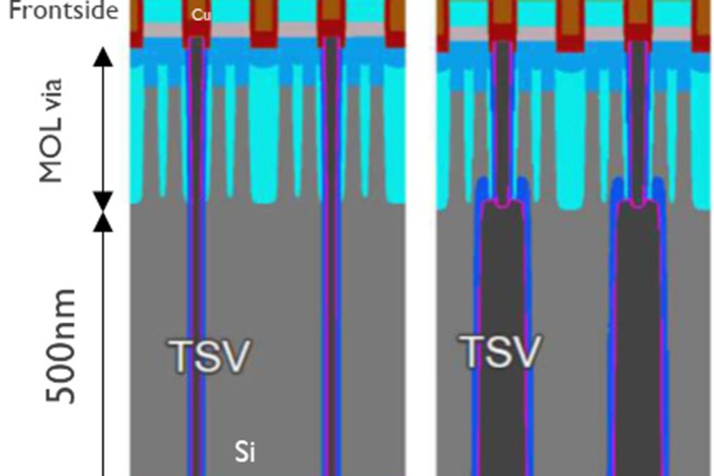
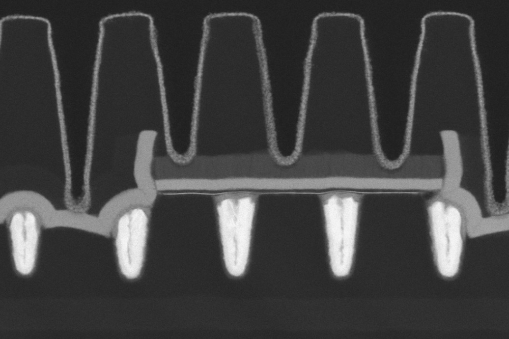
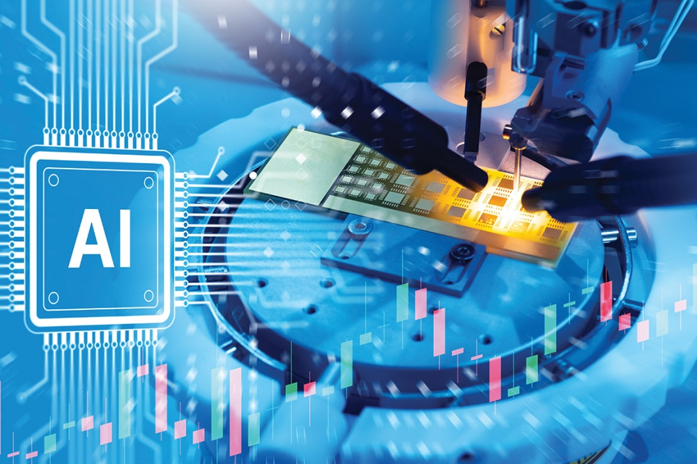
Scaling AI compute through advanced packaging
While transistor scaling remains essential, TSMC made it
clear that future performance gains will increasingly depend on
advanced packaging and system integration technologies.
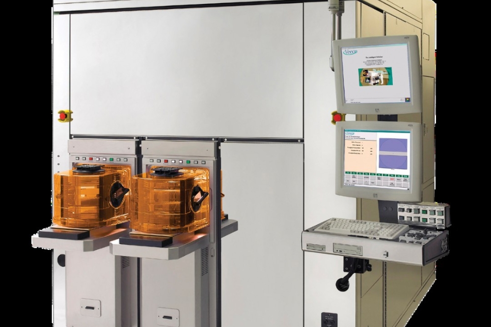
TSMC announced that it has achieved production of 5.5-reticle CoWoS packages with yields exceeding 98%, marking a significant milestone in manufacturability. Looking ahead, the company plans to scale CoWoS to 14-reticle configurations by 2028 and beyond 14 reticles by 2029, supporting up to 24 HBM stacks.
This scaling trajectory is remarkable, effectively enabling exponential increases in compute capability within a single package. The number of transistors integrated within these systems is expected to grow dramatically, further reinforcing the role of packaging as a key driver of performance.
Complementing CoWoS is TSMC’s System-on-Wafer (SoW) technology, which takes integration to an even higher level. SoW enables wafer-scale integration of logic and memory, with potential configurations supporting dozens of compute dies and up to 64 HBM stacks. The upcoming SoW-X platform, expected in 2029, is designed to meet the extreme demands of AI training workloads.
At the same time, TSMC continues to advance its SoIC (System-on-Integrated-Chips) technology, which provides high-density 3D stacking capabilities. Compared to traditional 2.5D approaches, SoIC offers significantly greater interconnect density and improved power efficiency. Future iterations are expected to achieve even tighter bonding pitches and higher performance.
Together, these technologies represent a shift towards system-level scaling, where performance gains are achieved not just through smaller transistors, but through more sophisticated integration of multiple components.

Photonics and the future of data movement
One of the most compelling areas of innovation highlighted
at the symposium was the integration of photonics into semiconductor systems.
TSMC’s Compact Universal Photonic Engine (COUPE) is designed to enable co-packaged optics (CPO), allowing optical communication components to be integrated directly into semiconductor packages. This approach addresses one of the key bottlenecks in AI systems: data movement.
Compared to traditional copper interconnects, CPO with COUPE offers dramatic improvements in both power efficiency and latency. Early implementations provide up to four times greater energy efficiency and a tenfold reduction in latency, with further gains expected as the technology matures.
The first production implementation, featuring a 200Gbps micro-ring modulator, is expected in 2026. Looking ahead, TSMC aims to scale the technology to support 400Gbps data rates and beyond, with bandwidth densities reaching approximately 4Tbps per millimetre by 2030.
These developments are critical for enabling large-scale AI systems, where the efficient movement of data between chips and across racks is becoming as important as compute performance itself.
Automotive, robotics and physical AI
The symposium also highlighted the growing importance of
what TSMC describes as “physical AI” — applications where AI systems interact
directly with the physical environment.
This includes autonomous vehicles, robotics and emerging applications such as humanoid robots. These systems require a combination of high-performance computing, real-time sensing, connectivity and power management, all integrated into highly reliable platforms.
TSMC is addressing these requirements with specialised
process technologies such as N3A and N2A, which are designed to meet stringent
automotive standards. The introduction of nanosheet-based automotive
processes marks a significant step forward, enabling higher performance and efficiency in safety-critical applications.
At the system level, physical AI platforms combine multiple semiconductor components, including application processors, microcontrollers, sensors and communication modules. The integration of these elements reflects the increasing complexity of modern electronics, where multiple domains converge within a single system.
The company also highlighted the role of silicon in enabling humanoid robotics, illustrating how sensing, computation and control functions come together to create intelligent machines capable of interacting with the real world.
Specialty technologies and broader innovation
Beyond leading-edge nodes, TSMC continues to invest in a
wide range of specialty technologies that support diverse applications.
In the RF domain, the company’s advanced CMOS technologies are enabling significant improvements in power efficiency and performance for wireless devices. These innovations are particularly relevant for emerging applications such as AI-enabled wearables and augmented reality (AR) systems.
Memory technologies are also evolving, with MRAM and RRAM playing an increasingly important role in next-generation designs. These non-volatile memory solutions offer advantages in scalability, performance and energy efficiency, making them well suited to both AI and embedded applications.
In display technologies, TSMC’s introduction of high-voltage FinFET processes represents a notable advancement, enabling more efficient and compact solutions for OLED displays and near-eye devices.
Together, these developments highlight the breadth of TSMC’s
innovation ecosystem, extending far beyond advanced logic nodes.
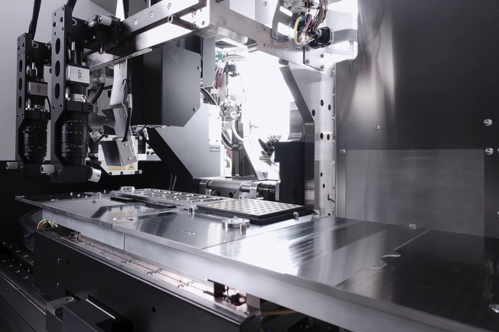
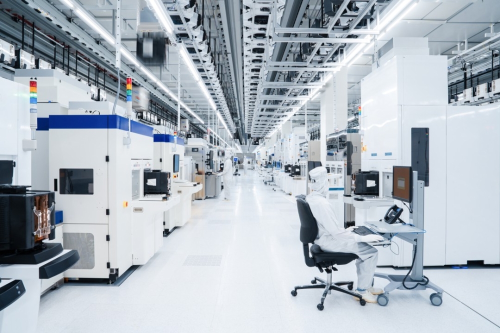
Manufacturing scale and sustainability
To support the surge in AI-driven demand, TSMC is
significantly expanding its manufacturing capacity. The company plans to build
nine new fab phases in 2026 alone, more than doubling its historical average.
Capacity for advanced nodes such as N2 and A16 is expected to grow rapidly, with a compound annual growth rate of approximately 70% between 2026 and 2028. At the same time, demand for AI-specific manufacturing, including large die wafers and advanced packaging, is increasing dramatically.
This expansion is underpinned by strong collaboration between research and development teams and manufacturing operations, enabling rapid scaling of new technologies.
Alongside capacity growth, TSMC is also focused on sustainability. The company has committed to achieving net-zero emissions by 2050 and is implementing initiatives in resource recycling and water stewardship. These efforts reflect the increasing importance of environmental considerations in semiconductor manufacturing.
Startups and ecosystem innovation
A notable feature of the symposium was the “Innovate with
TSMC” demo zone, which showcased emerging technologies from startup partners.
These included innovations in sensing, edge AI, connectivity and robotics.
These collaborations emphasise the role of TSMC not just as a manufacturer, but as an enabler of innovation across the broader semiconductor ecosystem. By providing access to advanced process technologies and design tools, the company is helping startups bring cutting-edge ideas to market.
Conclusion: A new era of system-level innovation
The 2026 Europe Technology Symposium made one thing
abundantly clear: the semiconductor industry is entering a period of
unprecedented growth and transformation.
AI is not just another application driving incremental demand; it is reshaping the entire landscape, from device architecture to system integration and manufacturing strategy. As AI evolves from generative models to physical systems, the demands placed on silicon will only continue to increase.
TSMC’s response is a comprehensive roadmap that spans advanced logic, packaging, photonics and system integration. At the same time, the company is scaling its manufacturing capabilities and strengthening its ecosystem to meet the needs of a rapidly changing industry.
The message from the symposium is ultimately one of convergence. Future performance gains will not come from any single innovation, but from the integration of multiple technologies across different layers of the stack.
In this new era, success will depend not just on transistor
scaling, but on the ability to orchestrate complex systems that bring together
compute, memory, connectivity and intelligence. TSMC’s roadmap suggests that it
is well positioned to lead this transformation, unleashing innovation at every
level of the semiconductor ecosystem.