Closing the gap: How intelligent sensing is reshaping wafer process control
With semiconductor fabs under increasing pressure to improve performance and maximize productivity, verifying critical tool conditions while minimizing downtime is becoming increasingly important. Here, Vidya Vijay, Director of Business Development at Nordson Test and Inspection, examines how intelligent in-situ sensing is helping manufacturers to achieve these objectives while supporting the wider shift toward more predictive semiconductor manufacturing
As semiconductor manufacturing advances into ever smaller nodes and more complex architectures, the margin for mechanical variation is rapidly diminishing. In modern fabrication environments, even the slightest deviation in wafer positioning or process geometry can translate into measurable differences in yield, reliability, and overall equipment effectiveness.
At the same time, fabs are under increasing pressure to maximize tool uptime, reduce operator dependency, and move toward more connected, autonomous production models, particularly as workforce constraints add growing pressure to reduce manual intervention. These competing demands expose the limitations of traditional setup and maintenance approaches, particularly where manual checks and operator judgement remain central.
In response, the industry is turning its attention to intelligent sensing technologies that align more closely with the precision demands of modern advanced semiconductor manufacturing.
Why modern process control demands a new approach
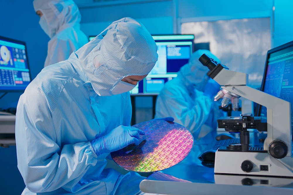
For decades, key setup and maintenance procedures in wafer processing have relied on manual intervention. Verifying wafer centreing, checking transfer accuracy, or measuring critical gaps between components has historically required tools to be taken offline, opened, and physically inspected. While long accepted, this approach introduces inherent inefficiencies. Maintaining vacuum integrity in production is not simply a matter of convenience, it is fundamental to process stability, as any interruption can introduce contamination risk, trigger cleaning cycles, and require time-intensive pump-down before production can resume. What begins as a routine check can rapidly evolve into extended and costly downtime.
Beyond this, manual procedures are often iterative and dependent on operator experience. Subtle differences in interpretation, sometimes as minute as tens of microns, can lead to meaningful variation in process outcomes. As fabs scale and process tolerances tighten, this variability becomes increasingly difficult to manage.
The growing importance of micron-level control
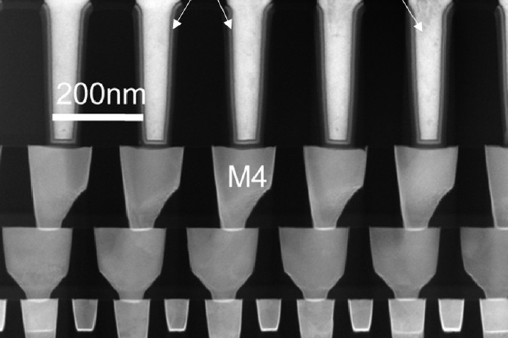
In advanced semiconductor processes, precise wafer positioning across X, Y, and Z axes is critical. Even minor deviations, particularly in vertical gap, can influence uniformity, contribute to edge defects, or introduce backside contamination. In more severe cases, misalignment can lead to wafer handling issues or unexpected tool alarms. In multi-chamber tools, the challenge extends further. It is not enough for each chamber to be accurate in isolation; they must also be matched to one another to ensure consistent results across production lots. Without this level of consistency, subtle variations can accumulate, impacting yield and complicating process optimization.

The implications can also be significant during recipe development, where engineers need confidence that any observed variation is driven by process chemistry rather than mechanical inconsistency. Without reliable measurement, isolating these factors becomes increasingly complex.
Measurement versus interpretation
One of the more understated challenges in traditional approaches is the reliance on visual feedback. In many cases, inspection methods provide only an image or qualitative indication of alignment, leaving interpretation to the operator. While useful, this still introduces subjectivity. One engineer may judge a deviation differently from another, and even small differences can be critical in high-precision processes. As a result, visualization alone is often insufficient to ensure repeatable outcomes.
The shift toward quantitative, in-situ measurement addresses this gap. By providing precise, repeatable data on wafer position and gap conditions – alongside real-time visual feedback – modern sensing technologies remove ambiguity from the process, enabling adjustments to be based on accurate and objective measurement rather than judgement.

Bringing measurement inside the process
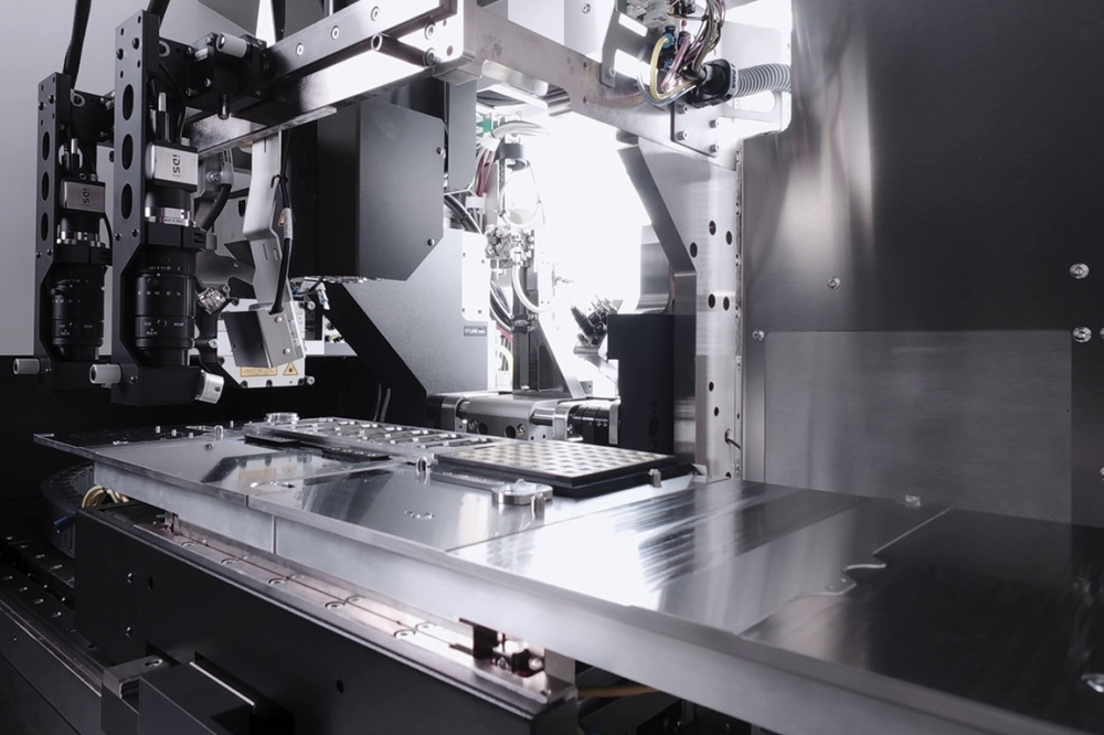
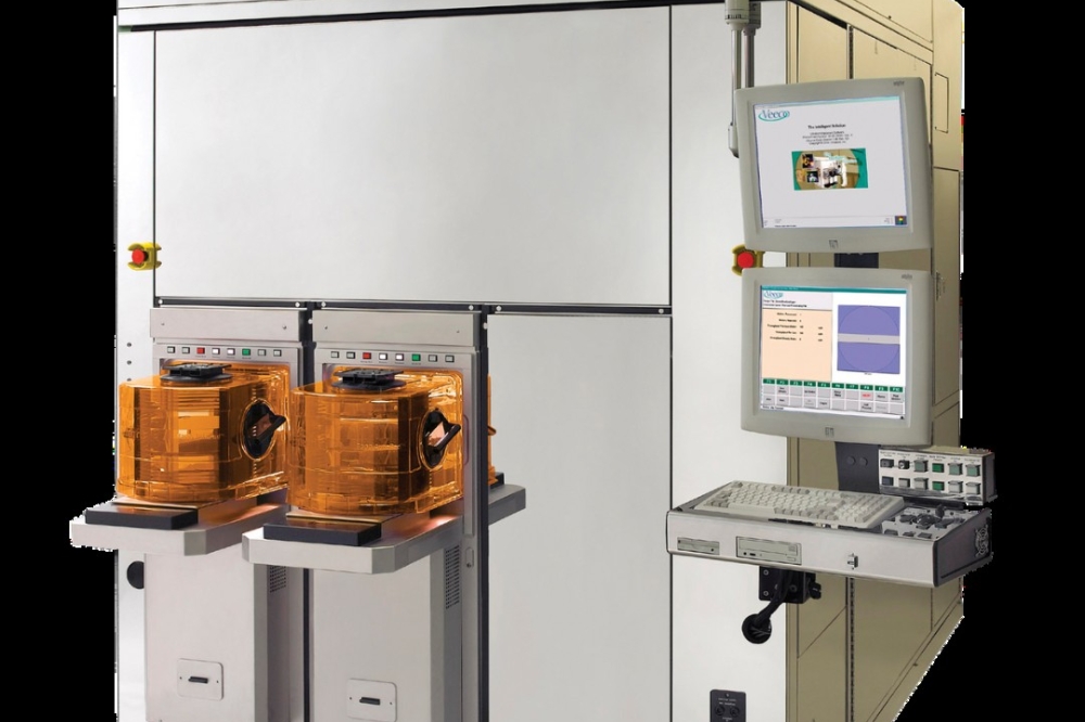
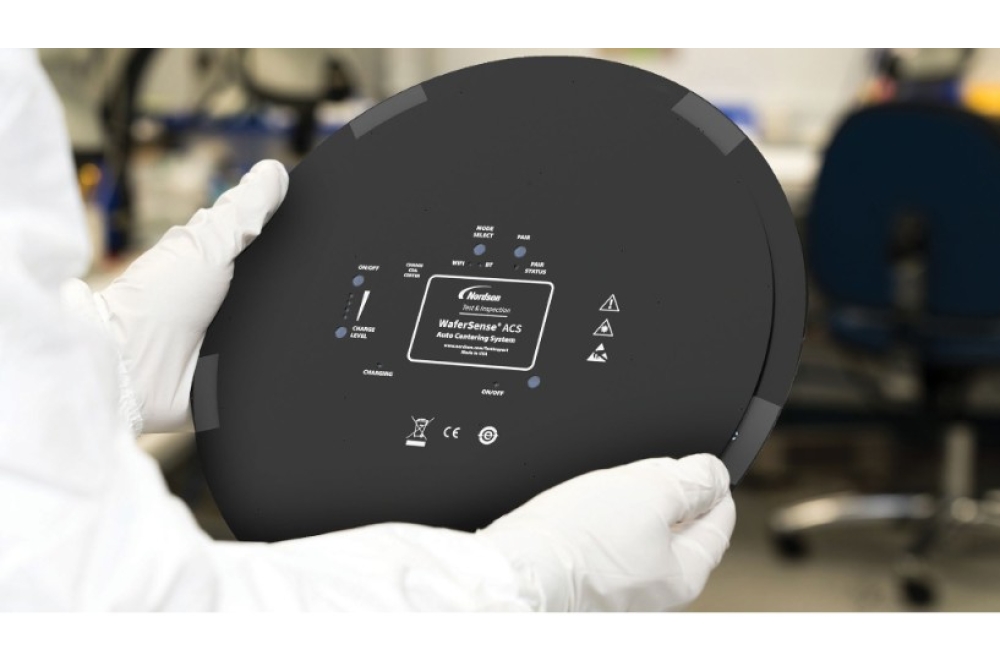
This need for greater precision and repeatability is driving adoption of advanced in-situ solutions. Nordson’s WaferSense® Auto Centering Sensor (ACS), for example, is designed to replicate the form of a production wafer and move through the tool path while capturing real-time X, and Y offset data for centre transfer positions without disassembly or requiring the equipment to be opened to ambient conditions.
By measuring under true process conditions, including vacuum, such systems provide a more accurate view of tool behaviour while preserving process integrity. They also deliver micron-level X, and Y data that can be applied to robot alignment, wafer handoff calibration, chamber setup and process optimisation, with far less downtime.
From preventative routines to predictive control
With access to real-time, in-situ measurement data, fabs are increasingly able to move beyond fixed preventative maintenance schedules. Traditionally, tools are serviced after a predefined number of wafer lots, regardless of their actual condition. While effective to a degree, this approach can result in both unnecessary intervention and missed early warning signs.
The more meaningful shift is not simply faster measurement, but a more informed basis for decision-making. When engineers have visibility on subtle changes in wafer positioning, gap conditions, or component wear as they emerge, maintenance becomes less about adhering to a fixed routine and more about responding to actual tool behaviour. This allows for earlier and more precise intervention, before variation begins to affect yield or develop into more serious and expensive failures.

Over time, this creates scope for a more refined maintenance strategy overall. Rather than relying on fixed schedules alone, fabs can make better-informed decisions about when maintenance is genuinely required, helping to reduce unnecessary disruption while maintaining tighter control over process consistency. This capability is particularly valuable when qualifying new process recipes, where both mechanical and chemical variables must be tightly controlled to ensure consistent results.
Keeping uptime up – and cost of disruption firmly down
In high-value semiconductor manufacturing, time is one of the most critical resources. Any reduction in maintenance duration has a direct impact on productivity, but the real gains come from minimizing disruption altogether. By eliminating the need for manual intervention and vacuum break procedures, in-situ sensing technologies can dramatically reduce setup and verification times. In some instances, processes that previously required several hours of intervention can be reduced to just minutes, allowing tools to return to production far more quickly. In the case of our own aforementioned Wafersense ACS, for example, we’re typically seeing reductions of 30 to 70 percent in setup time.
Equally important is the avoidance of more severe downtime events, particularly as with every hour that hardware is down, manufacturers can be exposed to significant financial cost ranging from tens of thousands to millions of dollars. A misaligned wafer or incorrect gap condition can lead to handling errors or, in extreme cases, wafer breakage within the tool. Recovery from such events can take days, involving cleaning, recalibration, and full process requalification. By improving measurement accuracy and reducing reliance on manual estimation, advanced sensing solutions help mitigate these risks, supporting more stable and predictable operation.
Software as the bridge to smarter manufacturing
As with many developments in semiconductor manufacturing, the hardware is only part of the story. The value of measurement lies in how effectively it can be interpreted and applied.
Real-time software platforms are playing an increasingly important role, providing live visibility into tool conditions and enabling immediate response. Engineers can monitor measurements as they are captured, diagnose issues more quickly, and make adjustments with greater confidence. What’s more, measurement data can be fed into automated workflows, supporting closed-loop control and enabling more connected, responsive manufacturing environments. This is a valuable evolution that reflects the industry’s wider move towards smarter production, predictive metrology and advanced, data-driven automation.
The quieter but critical shift shaping future success
While industry attention often focuses on major advances in electronics, some of the most impactful developments in manufacturing are, in fact, those that improve the precision and repeatability of the underlying processes. Intelligent wafer-based sensing represents precisely this type of shift, helping to close a long-standing gap in semiconductor manufacturing.
As fabs continue their progression toward greater automation and tighter tolerances, in step with the wider evolution of electronics, this ability to measure and act on real conditions in real time will become increasingly important. In an industry where success is measured in microns, and often fractions of them, access to this level of insight is no longer an optional refinement, it is a requirement for success.