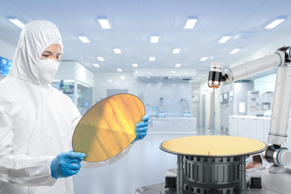
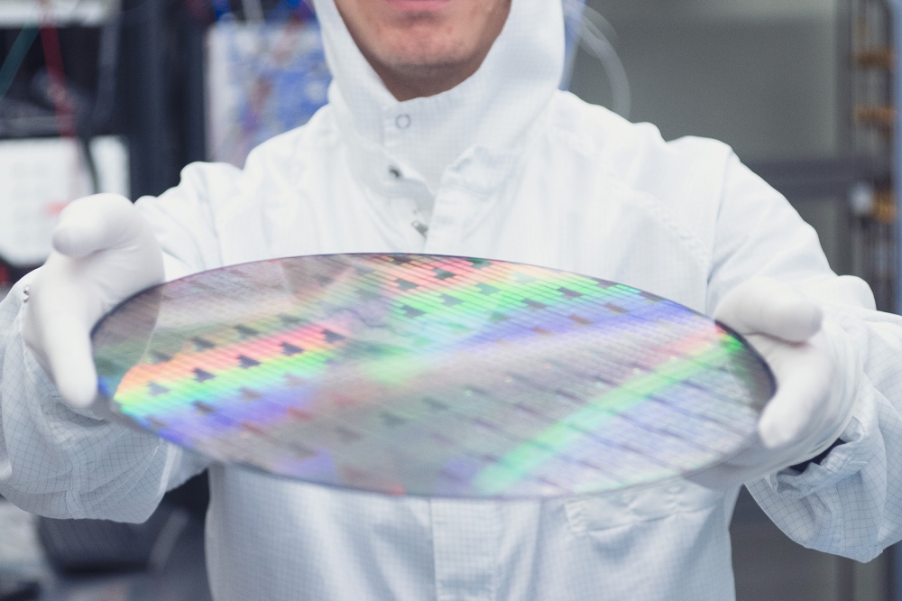
Advantest and Tokyo Seimitsu announce joint development of Die-Level Prober

Semiconductors are expected to become increasingly advanced and complex in the coming years. To promptly meet evolving market needs and deliver high-performance total test solutions to our customers, close collaboration across the semiconductor value chain is essential. Advantest and Tokyo Seimitsu will jointly develop die-level probers, leveraging their respective expertise to deliver advanced probing capabilities essential for testing AI and high-performance computing (HPC) devices.
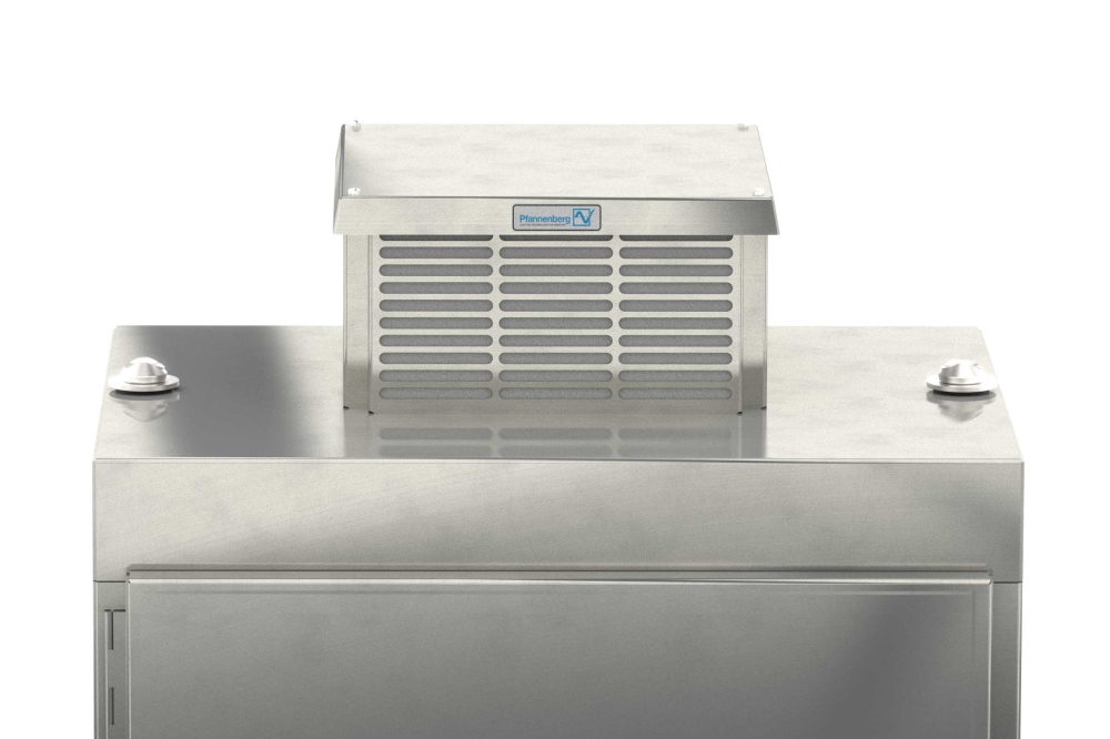
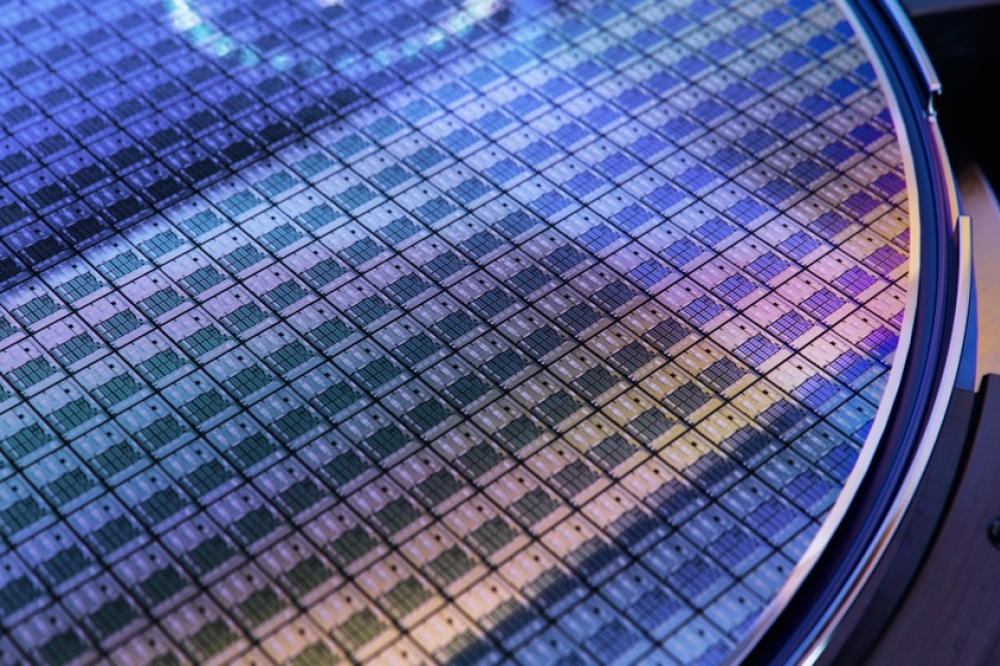
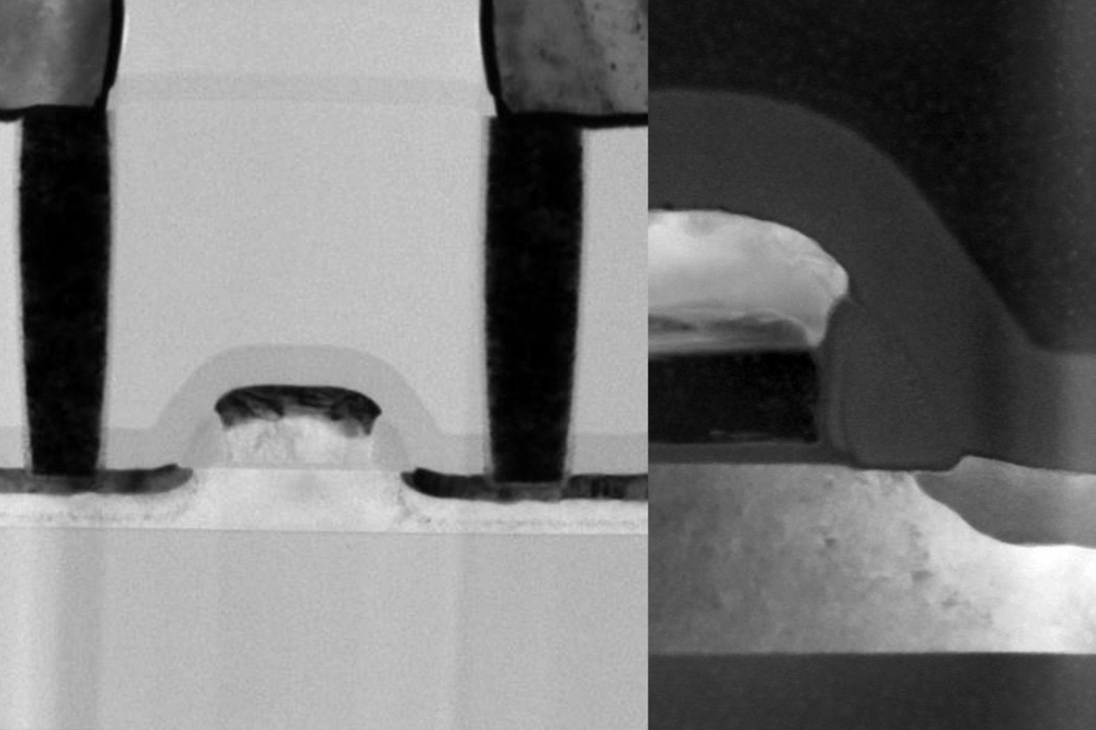
AI and high-performance computing (HPC) devices, such as GPUs and CPUs used in servers, require extremely high computational performance for AI model training, inference and execution. These devices often employ advanced 2.5D/3D packaging technologies, which generate significant heat during massive data processing. As a result, controlling temperature during test is a major challenge. Through this collaboration, the two companies will strengthen next-generation probing and handling technologies to address these challenges and contribute to the growth of the AI/HPC market.
“We offer various solutions centered on precision positioning technology in response to the advancement of AI/HPC technologies that are transforming the world. This collaboration will enable us to reach new heights of innovation as we work with Advantest to develop sophisticated die-level probing solutions that cater to the demands of the AI era,” said Ryuichi Kimura, President and CEO of Tokyo Seimitsu.
“We are actively pursuing partnerships with key players in the semiconductor value chain to address customer challenges in semiconductor testing, including the rapidly growing AI/HPC market,” said Douglas Lefever, Representative Director and Group CEO of Advantest. “Through our collaboration with Tokyo Seimitsu, we will deliver high-performance, comprehensive test solutions that meet our customers' future needs in areas of die-level probing.”